Method for chemical gaseous phase deposition of silicon nitride film by electron cyclotron resonance plasma

A technology of electron cyclotron resonance and chemical vapor deposition, which is applied in the field of microelectronics, can solve the problems of low deposition rate, poor uniformity of large area, high hydrogen content, etc., and achieve low deposition temperature, excellent uniformity and repeatability Effect

Inactive Publication Date: 2008-01-16
XIDIAN UNIV
View PDF0 Cites 7 Cited by
  • Summary
  • Abstract
  • Description
  • Claims
  • Application Information

AI Technical Summary

Problems solved by technology

[0007] The purpose of the present invention is to provide a method for electron cyclotron resonance plasma chemical vapor deposition of silicon nitride film, to overcome the high temperature preparation of existing silicon nitride film, low deposition rate, poor uniformity of large area and high hydrogen content Defects, realize the growth of silicon nitride film in the integrated circuit process as a diffusion barrier layer and device passivation layer or apply to some optical device manufacturing processes

Method used


Image

  • Method for chemical gaseous phase deposition of silicon nitride film by electron cyclotron resonance plasma
  • Method for chemical gaseous phase deposition of silicon nitride film by electron cyclotron resonance plasma
  • Method for chemical gaseous phase deposition of silicon nitride film by electron cyclotron resonance plasma

Examples


Embodiment 1

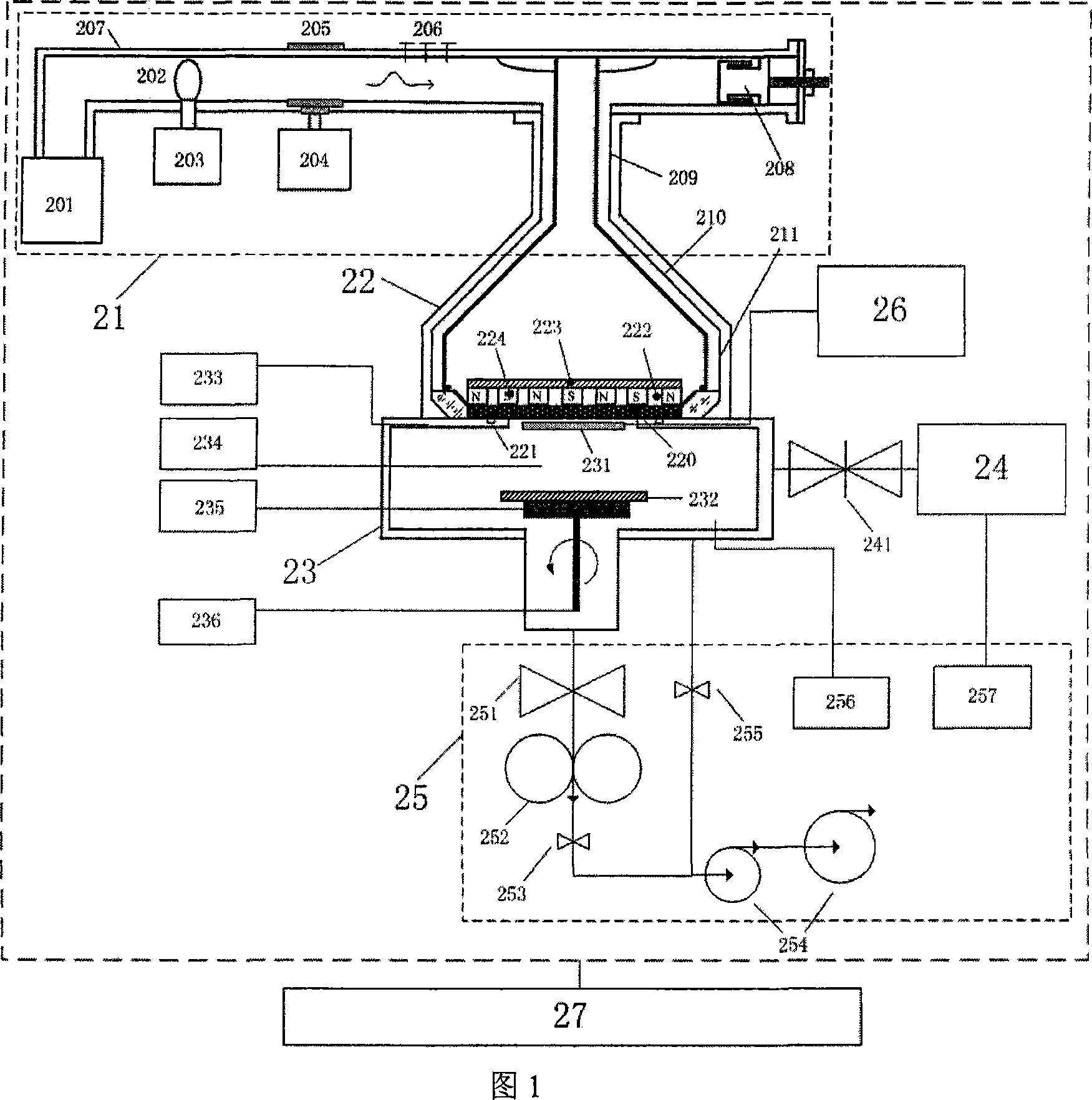
[0060] The present invention selects a p(100) single crystal silicon chip with a substrate size of Φ150mm as the substrate.

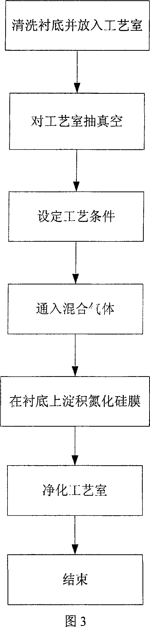
[0061] In the first step, the substrate is cleaned and placed in the process chamber.

[0062] Immerse the wafer in 4:1 H 2 SO 4 :H 2 o 2 The solution was cleaned for 10 minutes at a solution temperature of 90 ° C; the deionized water was cleaned for 5 minutes, including 6 cycles; the silicon wafer was immersed in 5:1:1 H 2 O:H 2 o 2 : Wash in HCl solution for 10 minutes at a solution temperature of 70°C; wash in deionized water for 5 minutes including 6 cycles; soak the wafer in a 50:1 HF solution for 15 to 30 seconds; wash in deionized water for 5 minutes including 6 cycles The second cycle: spin-drying treatment under the protection of nitrogen atmosphere, that is, washing with deionized water for 80 seconds, and spin-drying for 120 seconds. After cleaning, a clean silicon surface with a surface saturated by H-bonds is obtained. The cleaned s...

Embodiment 2

[0078] The present invention selects a p(100) single crystal silicon chip with a substrate size of Φ150mm as the substrate.

[0079] In the first step, the substrate is cleaned and placed in the process chamber.

[0080] Immerse the wafer in 4:1 H 2 SO 4 :H 2 o 2 The solution was cleaned for 10 minutes at a solution temperature of 90 ° C; the deionized water was cleaned for 5 minutes, including 6 cycles; the silicon wafer was immersed in 5:1:1 H 2 O:H 2 o 2 : Wash in HCl solution for 10 minutes at a solution temperature of 70°C; wash in deionized water for 5 minutes including 6 cycles; soak the wafer in a 50:1 HF solution for 15 to 30 seconds; wash in deionized water for 5 minutes including 6 cycles The second cycle: spin-drying treatment under the protection of nitrogen atmosphere, that is, washing with deionized water for 80 seconds, and spin-drying for 120 seconds. After cleaning, a clean silicon surface with a surface saturated by H-bonds is obtained. The cleaned s...

Embodiment 3

[0096] The present invention selects the quartz plate whose substrate is Φ10mm as the substrate.

[0097] In the first step, the substrate is cleaned and placed in the process chamber.

[0098] Wash the quartz sheet with acetone tidal sound for 20 minutes; wash with deionized water for 5 minutes including 6 cycles; spin dry treatment under the protection of nitrogen atmosphere, that is, wash with deionized water for 80 seconds, and spin dry for 120 seconds. The cleaned quartz wafer is placed on the sample stage 232 in the process chamber 23 .

[0099] The second step is to evacuate the process chamber.

[0100] Turn on the oil-free vacuum pump, molecular pump and related valves in sequence to evacuate the process chamber so that the background vacuum reaches 1.0×10 -5 Pa.

[0101] The third step is to set the process conditions respectively.

[0102] 1. The temperature of the substrate is set to 200°C;

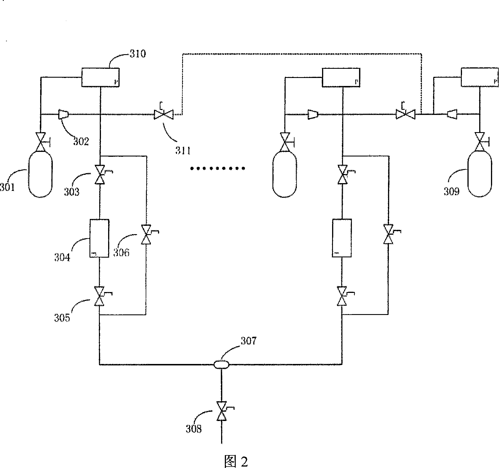
[0103] 2. The total gas flow rate is 150 sccm, and the gas flow rati...


PUM

PropertyMeasurementUnit
refractive indexaaaaaaaaaa

Abstract

The invention discloses a low-temperature manufacturing method of silicon nitride film used in passivation layer of an integrated circuit. The silicon nitride film grows on a substrate positioned inside a deposition chamber. The method comprises cleaning the substrate and placing inside the working chamber, vacuumizing the working chamber and presetting working conditions, introducing a mixed gas composed of silicon source gas and nitride source gas into the working chamber, performing ionization and decomposition of the mixed gas with the action of energy absorbed from a microwave source upon electron cyclotron resonance effect, transferring active charged particles produced by the ionization and decomposition to the surface of the substrate with the action of permanent magnetic field, and depositing silicon nitride film on the substrate. The working conditions are as follows: working chamber pressure: 0.1-5Pa, microwave power: 600-2000W, deposition temperature: room temperature to 300 DEG C, total gas flow: 50-300sccm, flow ratio of silicon source gas to nitride source gas: 1:6 to 1:12, and substrate rotation speed: 60 r/min. The inventive method can rapidly and uniformly deposit the low-hydrogen silicon nitride film (6 inch thickness) at low temperature (below 300 DEG C), which is used as a material for passivation layer of integrated circuit or optical devices.

Description

technical field [0001] The invention belongs to the technical field of microelectronics and relates to the manufacture of semiconductor integrated circuits, in particular to a low-temperature plasma chemical vapor deposition method for silicon nitride thin films used for passivation layers of integrated circuits. Background technique [0002] Silicon nitride material is one of the dielectric materials widely used in microfabrication technology. Silicon nitride has a high dielectric constant and refractive index, and can be used as the gate dielectric of metal-oxide-semiconductor MOS devices or used in the development or manufacturing process of optical devices; at the same time, silicon nitride also has a high density, It can effectively block the pollution of foreign impurities, and can be used as a diffusion barrier layer and a device passivation layer in the integrated circuit process. [0003] Silicon nitride films in integrated circuits are formed using known technique...

Claims


Application Information

Patent Timeline
Patent Type & Authority Applications(China)
IPC IPC(8): C23C16/511C23C16/52C23C16/34
Inventor 杨银堂吴振宇汪家友付俊兴柴常春
Owner XIDIAN UNIV
Why Eureka
Try Eureka