

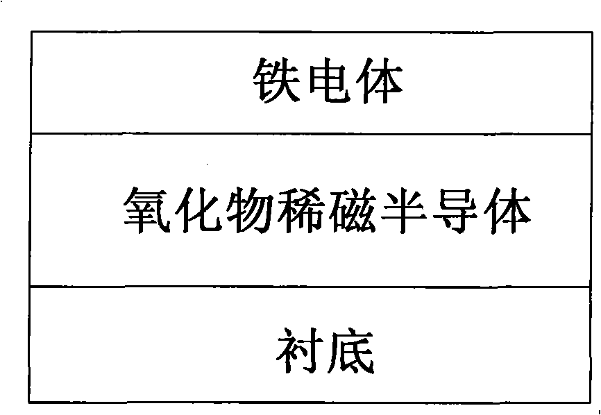
Oxide lanthanon magnetic semiconductor/ferroelectric heterogeneous structure and its making method
A technology of dilute magnetic semiconductor and heterostructure, applied in semiconductor/solid-state device manufacturing, semiconductor devices, circuits, etc., can solve problems such as non-volatile characteristics, improve integration and data storage capabilities, and have good application prospects Effect
- Summary
- Abstract
- Description
- Claims
- Application Information
AI Technical Summary
Problems solved by technology
Method used
Image

Examples
Embodiment 1
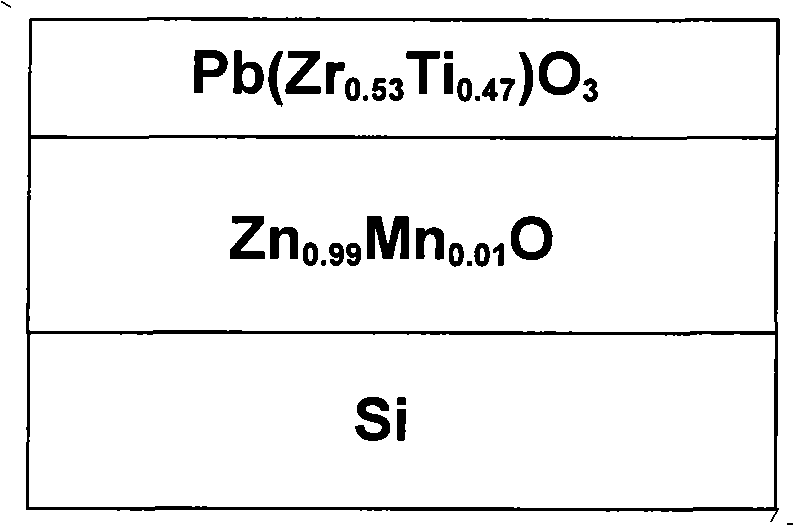
[0040] Example 1: Zn prepared by pulsed laser deposition 0.99 mn 0.01 O / Pb(Zr 0.53 Ti 0.47 )O 3 heterostructure, comprising the following steps:
[0041] (1) Target and substrate installation
[0042] In a vacuum chamber, the ZnO target material doped with manganese 1% and Pb(Zr 0.53 Ti 0.47 )O 3 The target is installed on a multi-target rack, and the Si substrate is cleaned and installed on the substrate rack, so that the direction of the laser beam is aligned with the manganese-doped ZnO target, and the distance between the substrate and the target is adjusted to 58mm.
[0043] (2) vacuuming
[0044] Turn on the mechanical pump and the molecular pump in turn to pump the pressure in the vacuum chamber to 1.5*10 -5 Pa.
[0046] Turn on the YAG solid-state laser (the laser wavelength is 532nm), adjust the energy of the single pulse of the laser to 230mJ, so that the energy density of the laser single pulse is 7J / cm 2 , the laser repetition ...
Embodiment 2
[0047] Embodiment 2: Sol-gel method prepares Sn 0.99 mn 0.01 o 2 / Pb(Zr 0.53 Ti 0.47 )O 3 Heterogeneous structure, the steps are as follows:
[0048] (1) Preparation of Sn 0.99 mn 0.01 o 2 sol
[0049] To analyze pure Sn(CHCOO) 4 2H 2 O and Mn(CHCOO) 2 4H 2 O is a precursor, it is dissolved in the mixture (solvent) of ethylene glycol methyl ether and diethanolamine and is made into the solution that 50ml concentration is 0.4mol / l, wherein the molar ratio of diethanolamine and tin is 1: 1, and then use The system was stirred at 90° C. for 5 hours with a magnetic stirrer to obtain a transparent sol. The sol was filtered, and then placed in a thermostat at a temperature of 50° C. for 1 day and set aside.
[0050] (2) Preparation of Pb(Zr 0.53 Ti 0.47 )O 3 sol
[0051] The raw materials used are analytically pure lead acetate, zirconium nitrate and tetrabutyl titanate. According to the molar ratio of zirconium and titanium of 53:47, the raw materials are dissolved...
Embodiment 3
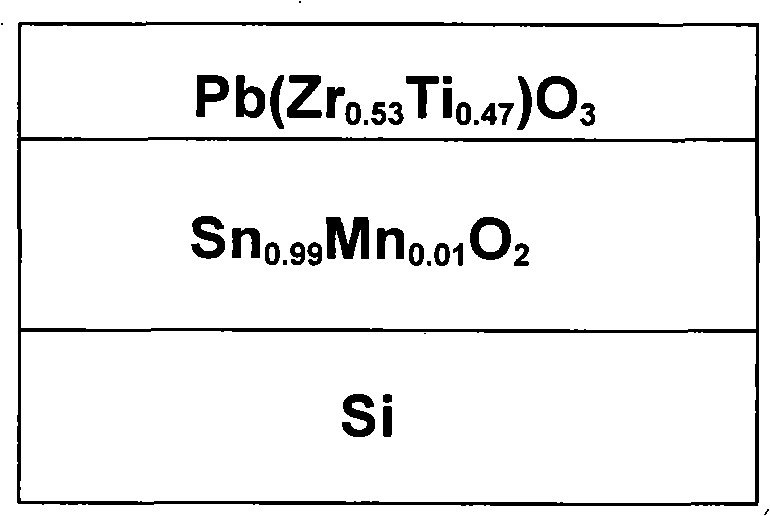
[0058] Embodiment 3: Preparation of Sn by pulsed laser deposition method 0.99 mn 0.01 o 2 / Pb(Zr 0.53 Ti 0.47 )O 3 Heterogeneous structure, the steps are as follows:
[0059] (1) Target and substrate installation
[0060] In a vacuum chamber, the manganese-doped 1% SnO 2 Target and Pb(Zr 0.53 Ti 0.47 )O 3 The target is installed on the multi-target rack, and the Si silicon substrate is cleaned and installed on the substrate rack, so that the direction of the laser beam is aligned with the manganese-doped SnO 2 For the target, adjust the distance between the substrate and the target to 55mm.
[0061] (2) vacuuming
[0062] Turn on the mechanical pump and the molecular pump in turn to pump the pressure in the vacuum chamber to 1.5*10 -5 Pa.
[0064] Then turn on the YAG solid-state laser, adjust the energy of the single pulse of the laser to 280mJ, so that the energy density of the laser single pulse is 10J / cm 2 , the laser repetition fre...
PUM
 Abstract
Description
Claims
Application Information