Process for preparing phase-change memory
A technology of phase-change memory and phase-change materials, which is applied in the field of microelectronics, can solve the problems of slow etching rate, etc., and achieve the effect of easy removal, easy realization, and promotion of development
- Summary
- Abstract
- Description
- Claims
- Application Information
AI Technical Summary
Problems solved by technology
Method used
Image
Examples
Embodiment 1
[0039] see Figure 1-Figure 9 , the present invention discloses a method for preparing a phase-change memory using high-density ordered self-assembled microspheres as a mask, combined with chemical mechanical polishing, which specifically includes the following steps:
[0040] [Step 1] Silicon wafer substrate cleaning.
[0041] Put the silicon chip into 1# liquid (a mixture of ammonia water, hydrogen peroxide, and deionized water, ammonia water: hydrogen peroxide: deionized water = 1:2:5) and boil for 5 minutes, cool, rinse with deionized water for 3 minutes, and then blow with nitrogen. Dry. Main function: remove oil and large particles on the silicon surface.
[0042] Put the silicon chip into 2# liquid (a mixture of hydrochloric acid, hydrogen peroxide, and deionized water, hydrochloric acid: hydrogen peroxide: deionized water = 1:2:5) to clean, the method is the same as the cleaning method of the above-mentioned 1# liquid; the main function is to remove Metal ions on th...
Embodiment 2
[0071] In this embodiment, the above-mentioned high-density ordered self-assembled microspheres are used as a mask, and the method for preparing a phase change memory in combination with chemical mechanical polishing includes the following steps:
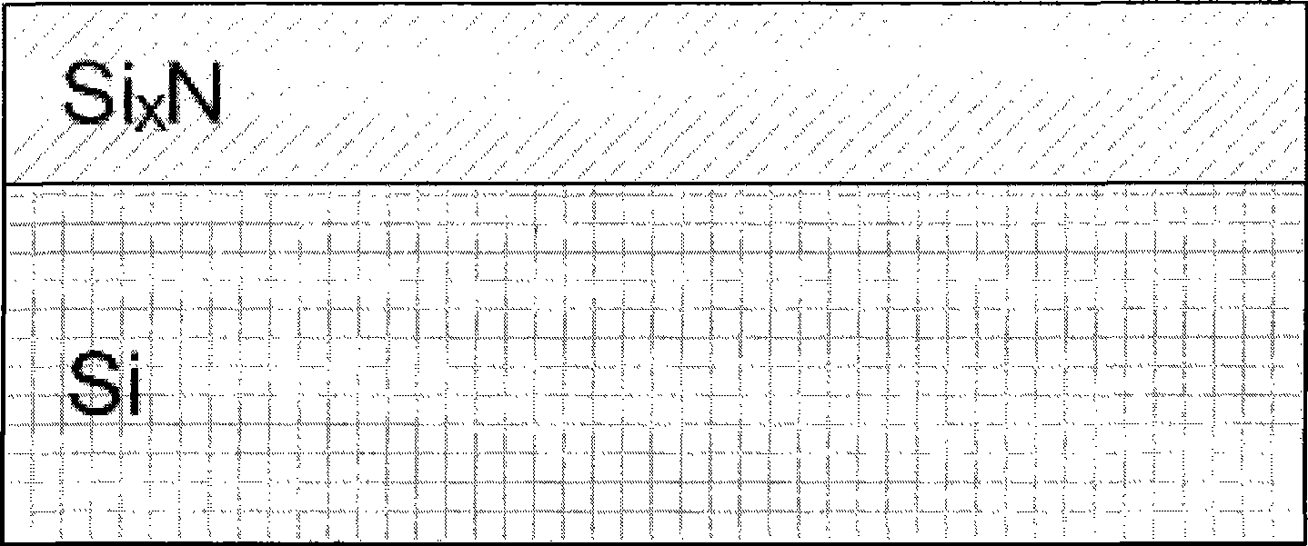
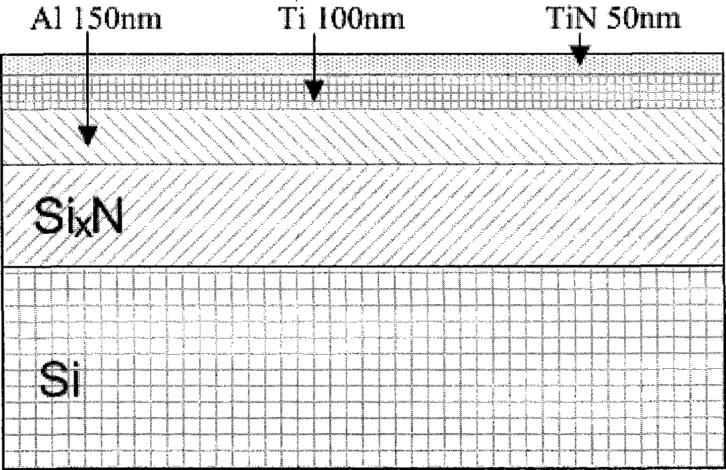
[0072] 1. On the (100)-oriented silicon wafer, a layer of SixN dielectric layer is first prepared by chemical vapor deposition, and its thickness is controlled to be 300-500nm;
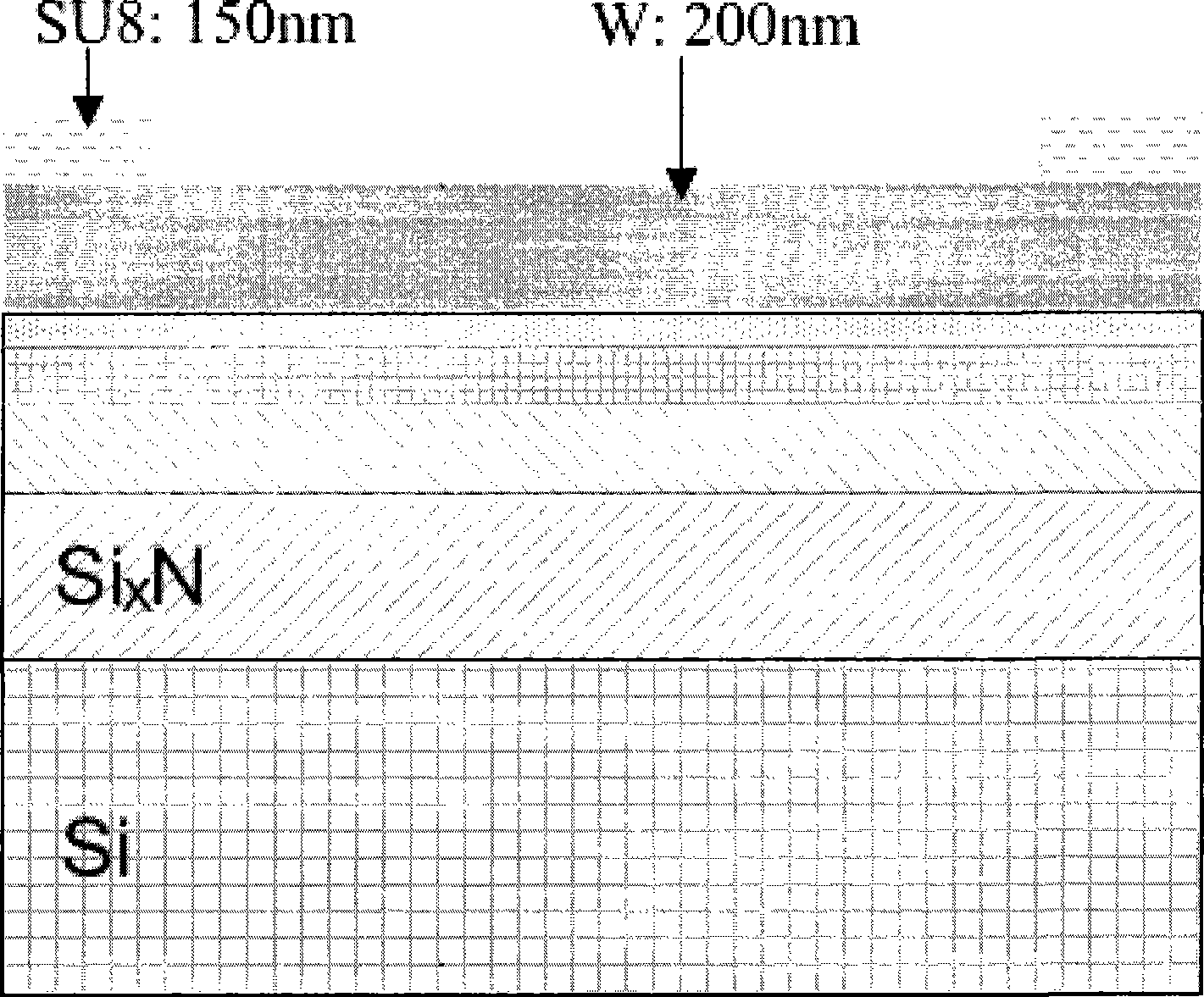
[0073] 2. Then use the method of magnetron sputtering to deposit 300nm thick Al / Ti / TiN, the corresponding thickness of each layer is 150nm / 100nm / 50nm, as the bottom electrode material, and magnetron sputtering 200nm thick metal tungsten on the bottom electrode material as marking layer material;
[0074] 3. Using electron beam lithography combined with reactive ion etching to form marking patterns as the basis for subsequent lithography alignment;
[0075] 4. Form a layer of photoresist pattern on the marking material by ultraviolet lithography to protect ...
PUM
| Property | Measurement | Unit |
|---|---|---|
| Thickness | aaaaa | aaaaa |
| Thickness | aaaaa | aaaaa |
| Line width | aaaaa | aaaaa |
Abstract
Description
Claims
Application Information


