Preparation technology of multi-purpose silicon micro-nano structure

A technology of micro-nano structure and nano-structure, applied in the field of new material technology and nano-materials, can solve the problems of reduced silicon nano-structure preparation efficiency, difficulty in large-area silicon micro-nano structure preparation, and increased cost.

Inactive Publication Date: 2009-09-23
BEIJING NORMAL UNIVERSITY
View PDF2 Cites 54 Cited by
  • Summary
  • Abstract
  • Description
  • Claims
  • Application Information

AI Technical Summary

Problems solved by technology

Although this technique can be applied to silicon substrates with different doping types, concentrations and orientations, and can control the length and crystallographic orientation of nanowires, it is difficult to obtain silicon nanowires with uniform diameter and orderly arrangement.
Our research group recently used polystyrene nanosphere and silica nanosphere template technology to prepare silicon nanowires with uniform diameter and order [Kuiqing Peng, Mingliang Zhang, Aijiang Lu, NingBew Wong, Ruiqin

Method used


Image

  • Preparation technology of multi-purpose silicon micro-nano structure

Examples


Embodiment 1

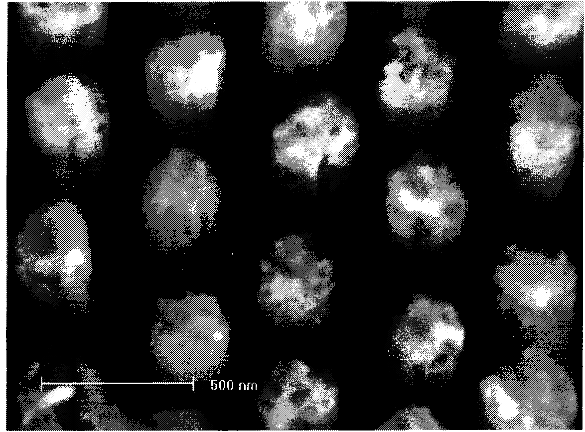
[0021] Coat photoresist on the clean silicon surface, and electron beam exposure will accurately copy the nanostructure pattern on the photolithographic mask on the clean silicon wafer surface coated with photoresist, and dissolve the unnecessary photoresist in the developing solution to obtain The resist-protected pattern required for etching has a line width of 100nm. After using high vacuum thermal evaporation technology to deposit a layer of 50nm thick metal silver film on the surface of the treated silicon wafer, the silicon wafer is soaked in the photoresist stripping solution, and the resist on the surface of the silicon wafer is covered on it. silver film removal. Immediately thereafter the wafer was immersed in HF+H 2 o 2 +H 2 O corrosion solution in a closed container, 25 degrees Celsius for 10 minutes. An array of silicon nanostructures is obtained. The samples were then soaked in concentrated nitric acid solution for at least one hour to remove the silver film...

Embodiment 2

[0023] Coat photoresist on the clean silicon surface, and electron beam exposure will accurately copy the nanostructure pattern on the photolithographic mask on the clean silicon wafer surface coated with photoresist, and dissolve the unnecessary photoresist in the developing solution to obtain The resist-protected pattern required for etching has a line width of 200nm. After using high vacuum thermal evaporation technology to deposit a layer of 50nm thick metal silver film on the surface of the treated silicon wafer, the silicon wafer is soaked in the photoresist stripping solution, and the resist on the surface of the silicon wafer is covered on it. silver film removal. Immediately thereafter the wafer was immersed in HF+H 2 o 2 +H 2 In an airtight container of O etching solution, treat at 25 degrees Celsius for 10 minutes to obtain a silicon nanostructure array. The samples were then soaked in concentrated nitric acid solution for at least one hour to remove the silver ...

Embodiment 3

[0025] Coat photoresist on the clean silicon surface, and electron beam exposure will accurately copy the nanostructure pattern on the photolithographic mask on the clean silicon wafer surface coated with photoresist, and dissolve the unnecessary photoresist in the developing solution to obtain The resist-protected pattern required for etching has a line width of 800nm. After depositing a 100nm-thick metal silver film on the surface of the treated silicon wafer using high vacuum thermal evaporation technology, the silicon wafer is soaked in a photoresist stripping solution, and the resist on the surface of the silicon wafer is covered on it. silver film removal. Immediately thereafter the wafer was immersed in HF+H 2 o 2 +H 2 In an airtight container of O etching solution, treat at 25 degrees Celsius for 10 minutes to obtain a silicon nanostructure array. The samples were then soaked in concentrated nitric acid solution for at least one hour to remove the silver film on th...


PUM


Abstract

The invention relates to a preparation technology of a multi-purpose silicon micro-nano structure, and belongs to the preparation technology field of new materials. A preparation method of a large-area highly-orderly silicon micro-nano structure array is researched though the combination of the metal-catalyzed silicon corrosion technology and the photoetching technology. A micro structure image on a photoetching mask plate is accurately copied to the surface of a clean silicon chip coated with a photoresist by utilizing an electron beam or ultraviolet light and other exposure technologies so as to obtain the image required during the corrosion process and protected by etching resist. A metal silver film is deposited on the surface of the silicon chip after the surface of the silicon chip is processed by utilizing high-vacuum heat-evaporation and other technologies; after the etching resist coated on the surface of the silicon chip and the silver film coated on the resist are removed, the silicon chip is immerged into a closed container of hydrofluoric acid corrosion solution containing an oxidant and processed for 10 to 100 minutes so as to obtain the large-area highly-orderly silicon micro-nano structure array. The large-area highly-orderly silica micro-nano structure array has wide application prospect in the fields of solar batteries, lithium battery cathode materials, gas sensors, active surface reinforced Raman spectrometry substrate and the like.

Description

technical field [0001] The invention relates to a multi-purpose ordered silicon micro-nano structure preparation technology, which belongs to the field of new material technology and nanometer materials. Background technique [0002] Due to their unique structure and physical properties, semiconductor micro-nanostructure materials have broad application prospects in nano-optoelectronics and new solar cell devices. Due to the important position of silicon materials in the traditional microelectronics industry, the research of one-dimensional silicon nanowires has received great attention. The current nano-silicon wire preparation methods mainly include chemical vapor deposition and oxide-assisted growth techniques. Due to the limitations of the growth mechanism, these methods usually require relatively high temperatures and some complicated equipment, resulting in high production costs. For example, the silicon wire growth temperature in patent 00117242.5 is as high as 1600...

Claims


Application Information

Patent Timeline
IPC IPC(8): H01L31/18G01N21/00H01M4/04H01M14/00H01G9/04H01G9/20B82B3/00
CPCY02E60/12Y02E60/10Y02P70/50
Inventor 彭奎庆王新
Owner BEIJING NORMAL UNIVERSITY
Why Eureka
Try Eureka