Capacitance structure and preparation method of a hybrid nanocrystalline memory

A nanocrystal and memory technology, applied in semiconductor/solid-state device manufacturing, circuits, electrical components, etc., to achieve the effects of inhibiting chemical reactions, good chemical stability and thermal stability, and improving storage density

Inactive Publication Date: 2011-12-14
FUDAN UNIV
View PDF3 Cites 0 Cited by
  • Summary
  • Abstract
  • Description
  • Claims
  • Application Information

AI Technical Summary

Problems solved by technology

In addition, the selection of electrodes in the preparation of capacitor storage will also greatly affect the performance of the device. Traditional polysilicon electrode materials have many problems such as high resistivity and low work function, which have great limitations in the application of nanocrystalline storage capacitors. The metal palladium electrode has a large work function (5.22eV), which can form a barrier height that is conducive to charge erasure with the capacitor medium, and palladium has good chemical stability and thermal stability, so it is used in nanocrystalline storage capacitors. It has great application prospects in the preparation of

Method used


Image

  • Capacitance structure and preparation method of a hybrid nanocrystalline memory
  • Capacitance structure and preparation method of a hybrid nanocrystalline memory
  • Capacitance structure and preparation method of a hybrid nanocrystalline memory

Examples


Embodiment 1

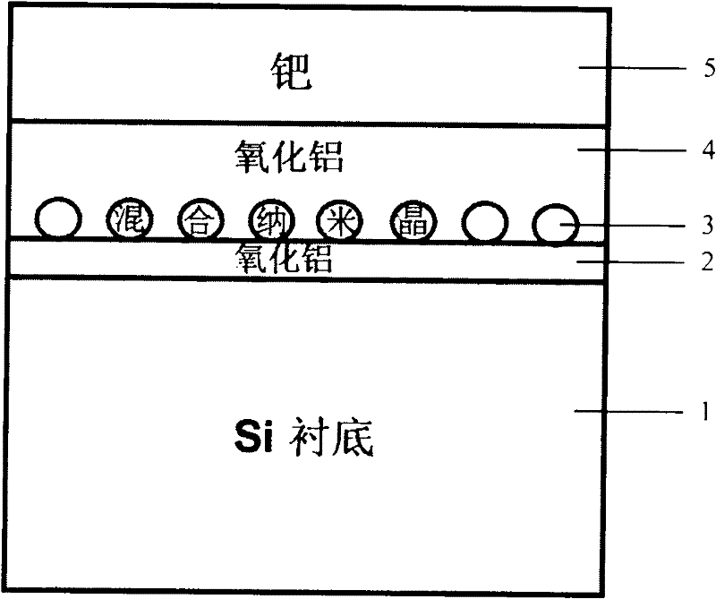
[0036] The following is an example of preparing ruthenium and ruthenium oxide mixed nanocrystal storage capacitors by adopting the storage capacitor structure and preparation method provided by the present invention.

[0037] A P-type single crystal silicon chip with (100) crystal orientation is used as a substrate, and the resistivity of the silicon chip is 8-12 ohm·cm. After the silicon wafer has undergone standard cleaning, it is placed in an atomic layer deposition system, and then the surface of the silicon wafer is modified with trimethylaluminum gas for 60 minutes at a temperature of 300°C. Al was then grown by atomic layer deposition 2 o 3 Nano film as tunneling layer, Al 2 o 3 The thickness is 9 nm. Next, magnetron sputtering a ruthenium metal film with a thickness of 2 nanometers on the tunneling layer, and then rapid thermal annealing at 800° C. for 30 seconds in a mixed atmosphere of nitrogen and trace oxygen to form mixed nanocrystals of ruthenium and rutheniu...


PUM

PropertyMeasurementUnit
thicknessaaaaaaaaaa
thicknessaaaaaaaaaa
thicknessaaaaaaaaaa

Abstract

The invention belongs to the technical field of semiconductor integrated circuit manufacturing, in particular to a capacitor of a nano-crystal memory and a preparation method thereof. The capacitor uses P-type single crystal silicon as a substrate, on which there are Al2O3 tunneling layer, ruthenium and ruthenium oxide mixed nanocrystal, Al2O3 barrier layer and palladium electrode layer. Among them, the Al2O3 layer is prepared by the atomic layer deposition method. The mixed nanocrystals are first deposited by magnetron sputtering to deposit the metal ruthenium layer, and then formed after rapid thermal annealing in a mixed atmosphere composed of nitrogen and trace oxygen. The palladium electrode layer is formed by lift -off method formation. The memory capacitance structure of the present invention has excellent characteristics such as good programming and erasing properties, long charge retention time, etc., and has good application prospects in flash memories.

Description

technical field [0001] The invention belongs to the technical field of semiconductor integrated circuit manufacturing, and in particular relates to a capacitor structure and a preparation method of a flash memory, in particular to a hybrid nanocrystal storage capacitor structure and a preparation method. Background technique [0002] With the continuous development of semiconductor process technology, the integration density of non-volatile flash memory is getting higher and higher, and the size of memory cells is reduced accordingly. After the 65nm technology node, the traditional polysilicon floating gate structure has a series of problems, which greatly It affects the performance of device storage, such as slow erasing and writing speed, high working voltage, etc. [1]. A new generation of non-volatile memory based on a discontinuous charge trapping mechanism (such as nanocrystalline memory, etc.) has recently attracted widespread attention. Compared with traditional poly...

Claims


Application Information

Patent Timeline
Patent Type & Authority Patents(China)
IPC IPC(8): H01L29/92H01L21/02H01L21/3205H01L21/321H01L21/316
Inventor 丁士进苟鸿雁
Owner FUDAN UNIV
Why Eureka
Try Eureka