Method for synthesizing carbide nano powder by solid-phase reaction
A technology of nano-powder and carbide, applied in the direction of carbide, tungsten/molybdenum carbide, etc., can solve the problems of gas pollution, etc., and achieve the effect of mild reaction pressure, lower reaction temperature and mild reaction temperature
- Summary
- Abstract
- Description
- Claims
- Application Information
AI Technical Summary
Problems solved by technology
Method used
Image
Examples
Embodiment 1
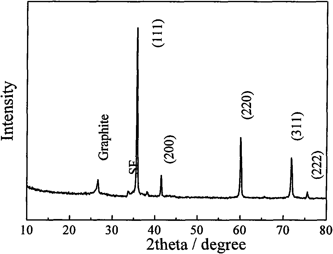
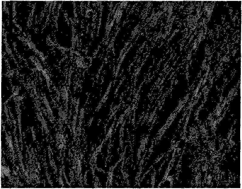
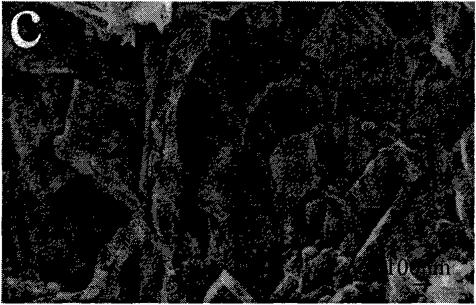
[0041] Silicon powder 1.4g, glucose 1.4g, Mg powder 1.5g and elemental iodine I 2 6g mixed, sealed in a 20mL stainless steel reaction kettle, reacted at a temperature of 120°C for 12 hours, after natural cooling, the resulting off-white powder was collected and washed with hydrochloric acid and deionized water respectively, and washed with a mixture of hydrofluoric acid and dilute nitric acid Excessive silicon powder, then the resulting product is washed with distilled water and absolute ethanol to neutral pH and then dried to obtain silicon carbide powder. The analytical spectrum of the product is as follows Figure 1-4 shown. figure 1 It is the XRD diffraction pattern of the obtained silicon carbide product, which corresponds to the standard card value (JCPDS no.29-1129). figure 2 It is a scanning electron microscope photo of the obtained silicon carbide nanowire, it can be seen that its diameter is about 65 nm, and its length is about several microns. image 3 It is a sc...
Embodiment 2
[0044] As described in Example 1, the difference is that 1.4 g of glucose is replaced by 1.4 g of maltose. Figure 5 is the XRD spectrum of the resulting product. 3C-SiC (JCPDS no.29-1129) can be calibrated as cubic crystal system.
Embodiment 3
[0046] Vanadium pentoxide (V 2 o 5 ) 0.43g, magnesium powder 0.551g, I 2 1.215g, glucose 0.14g mixed, sealed in a 20mL stainless steel reactor. The reaction time was 6 hours at 250°C. After washing, separating and drying, the XRD spectrum of the product obtained is as follows: Image 6 , can be calibrated as VC of the face-centered cubic system, which is in good agreement with the standard card (JCPDSno.65-8074). Figure 7 Its transmission electron micrograph shows that the obtained material is nanoscale. Figure 8 The photo of its high-resolution transmission electron microscope shows that its interplanar spacing is 0.204nm, which is in good agreement with the (002) plane of VC.
PUM
 Abstract
Description
Claims
Application Information


