Method for coarsening surface of light-emitting diode (LED) with the aid of metal nanoparticles

A metal nanoparticle, light-emitting diode technology, applied in metal material coating process, liquid chemical plating, coating and other directions, can solve problems such as unfavorable commercial application, poor controllability, complex process, etc. Production cost, the effect of improving extraction efficiency

Inactive Publication Date: 2011-08-31
SHANDONG UNIV
View PDF4 Cites 21 Cited by
  • Summary
  • Abstract
  • Description
  • Claims
  • Application Information

AI Technical Summary

Problems solved by technology

This invention reduces the waveguide loss inside the device by introducing a multi-layer structure, but the cost of making a thin film is greatly increased due to the multi-layer structure, which is not conducive to commercial applications, and the production of a multi-layer structure is difficult to guarantee the electrical performance
[0011] To sum up, in the past, the r...

Method used


Image

  • Method for coarsening surface of light-emitting diode (LED) with the aid of metal nanoparticles
  • Method for coarsening surface of light-emitting diode (LED) with the aid of metal nanoparticles
  • Method for coarsening surface of light-emitting diode (LED) with the aid of metal nanoparticles

Examples


Embodiment 1

[0038] Taking the epitaxial wafer of gallium nitride-based blue light-emitting diode as an example to illustrate the implementation method of the present invention:

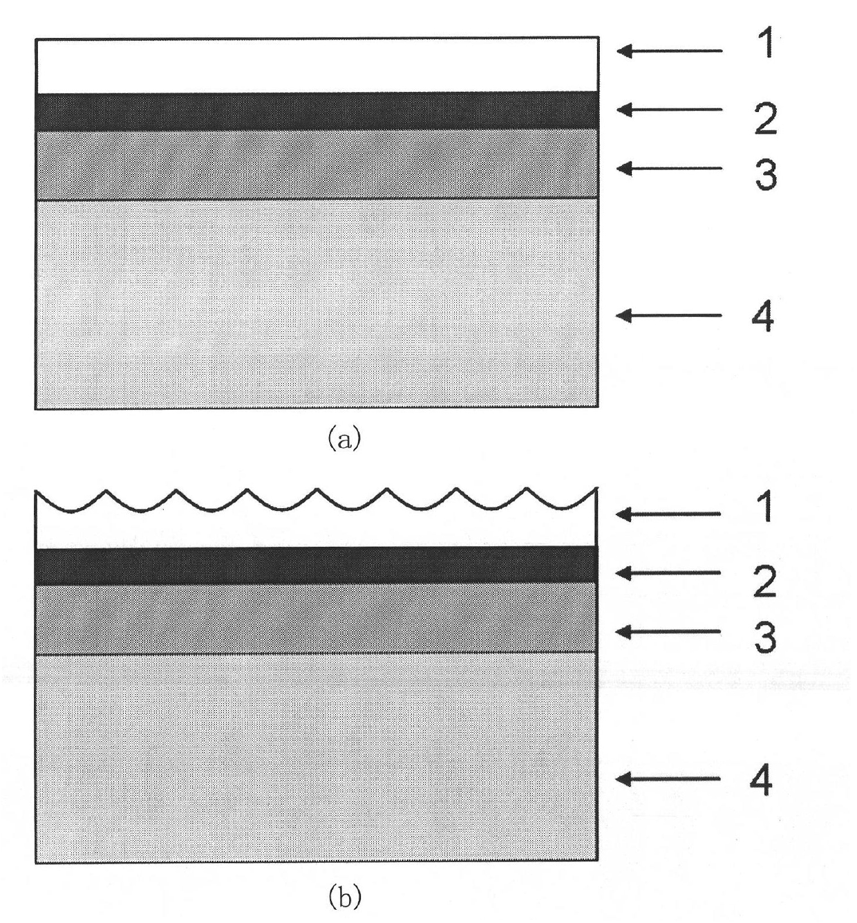
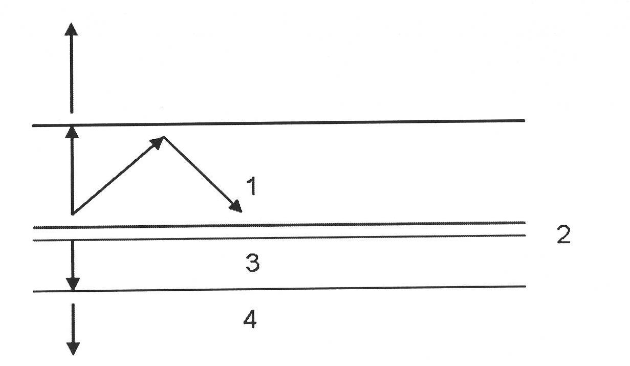
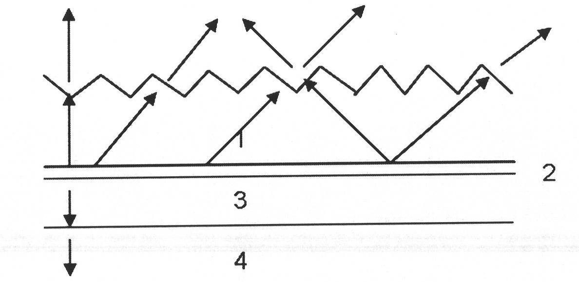
[0039] (1) On a substrate such as sapphire or silicon carbide, a buffer layer, N-GaN layer, active layer, and P-type gallium nitride layer are sequentially grown by metal-organic vapor deposition to form a gallium nitride-based light-emitting diode blue epitaxial wafer.

[0040] (2) The thickness of P-type gallium nitride is controlled to be 200nm-400nm.

[0041] (3) configure silver nitrate solution, the molar concentration of silver nitrate solution is between 0.M-1M, adopt deionized water to dissolve.

[0042] (4) Immerse the gallium nitride-based blue light epitaxial wafer in the silver nitrate solution, and deposit a layer of nano-silver on the surface of p-gallium nitride by ultraviolet light. The intensity of ultraviolet light is between 20W-100W, and the size of silver nanoparticles is 100nm-1000nm, the ...

Embodiment 2

[0051] Taking the epitaxial wafer of gallium nitride-based blue light-emitting diode as an example to illustrate the implementation method of the present invention, it is the same as in embodiment 1, except that in step (3), the metal salt solution used is potassium chloroplatinate, and then The gallium nitride-based blue light epitaxial wafer is immersed in the metal salt solution, and a layer of platinum is deposited on the surface of P gallium nitride by ultraviolet light. The intensity of ultraviolet light is between 20W-100W, and the size of platinum nanoparticles is 100nm-1000nm. The time of light irradiation is from 5min to 30min. Then adopt the same steps (5)-(11) as in Example 1 to configure the etching liquid, the etching liquid is selected hydrofluoric acid, the oxidizing agent is selected potassium bisulfate, and the mass concentration of the hydrofluoric acid solution is 10%-40 %, the molar concentration of potassium bisulfate is 0.05M-0.1M, and it is diluted with...

Embodiment 3

[0054] In this embodiment, red light AlGaInP light-emitting diodes are etched. The top layer structure of this light-emitting diode epitaxial wafer is a layer of P-GaP with a thickness of 10 μm. The metal salt solution configured is chloroauric acid or other metal salts. The epitaxial wafer is immersed in the metal salt solution, and a layer of metal nanoparticles can be deposited on the GaP surface without ultraviolet light. The size of the metal nanoparticles is 10nm-200nm. Then adopt the same steps (5)-(11) as in Example 1, hydrofluoric acid is selected for the corrosion solution, potassium bisulfate is selected for the oxidant, the mass concentration of the hydrofluoric acid solution is 10%-40%, and the mole of potassium bisulfate The concentration is 0.05M-0.1M, put the epitaxial wafer deposited with metal nanoparticles into the etching solution, and use ultraviolet light to irradiate for wet etching. The etching time is about 10min-60min, and the etching time is selected ...


PUM

PropertyMeasurementUnit
Thicknessaaaaaaaaaa

Abstract

The invention discloses a method for coarsening a surface of a light-emitting diode (LED) with the aid of metal nanoparticles, belonging to the technical field of manufacture of semiconductor optoelectronic materials and devices. The method comprises the steps: firstly, growing an LED epitaxial wafer on a semiconductor substrate, wherein the LED epitaxial wafer sequentially comprises an N-GaN film, a quantum well layer and a P-GaN layer; then depositing a layer of metal nanoparticles on the surface of the P-GaN layer with the aid of ultraviolet light in the solution of metal salts; placing the LED epitaxial wafer after being deposited with the metal nanoparticles in an etchant solution made from a certain proportion of hydrofluoric acid and oxidant; and performing wet etching with the aid of ultraviolet light. By depositing the metal nanoparticles on the N-GaN film, the electron distribution on the surface of the N-GaN film can be changed, the etching rate is increased, thereby being favorable to forming of a coarsened structure. The method disclosed by the invention is suitable for etching of different semiconductor materials and coarsening of the LED epitaxial wafer; and compared with the prior art, the cost is low, the coarsened area is large, the operation is simple, and an ideal coarsened effect can be obtained.

Description

Technical field: [0001] The invention relates to a method for realizing surface roughening of light-emitting diodes assisted by metal nanoparticles, and belongs to the technical field of semiconductor optoelectronic materials and device preparation. Background technique: [0002] In the past two decades, light-emitting diode (LED) technology has been significantly developed, especially LED technology based on gallium nitride materials by leaps and bounds. It makes LEDs commercially applied in display technology, lighting technology and other fields regularly. With the improvement of LED efficiency, the use of white LEDs to replace fluorescent bulbs will become a reality in the not-too-distant future. [0003] There are two ways to improve LED efficiency: one is to improve the internal quantum efficiency, and the other is to improve the extraction efficiency to further improve the external quantum efficiency. The internal quantum efficiency is mainly determined by the film ...

Claims


Application Information

Patent Timeline
IPC IPC(8): H01L33/00H01L33/20C23C18/42
Inventor 王瑞军刘铎左致远于谦徐现刚
Owner SHANDONG UNIV
Why Eureka
Try Eureka