A method for constructing microelectronic devices through hierarchical heterostructure nanomaterials

A technology of microelectronic devices and heterogeneous structures, applied in the fields of electrical components, semiconductor/solid-state device manufacturing, circuits, etc., can solve the problems of life and stability that cannot meet the needs of the electronics industry, the application and development of low electron mobility, and complex processing processes and other issues, to achieve the effect of easy promotion and application, low production cost and good repeatability

Inactive Publication Date: 2011-12-28
JILIN UNIV
View PDF3 Cites 7 Cited by
  • Summary
  • Abstract
  • Description
  • Claims
  • Application Information

AI Technical Summary

Problems solved by technology

According to the type of material, it can be divided into non-field effect transistors and organic field effect transistors. Although organic field effect transistors have great advantages over non-field effect transistors in terms of price, flexibility, device fabrication and operation, they have lower electron mobility. (Generally within 0.01cm 2 / Vs or less) has become a bottleneck restricting its real application and development
In addition, the existing organic and non-field effect transistors cannot meet the needs of the current electronics industry in terms of life and stability, and further improvement is needed.
Moreover, the previous methods sometimes require complicated processing, which will increase the degree of craftsmanship and increase the price, which is not conducive to popularization

Method used


Image

  • A method for constructing microelectronic devices through hierarchical heterostructure nanomaterials
  • A method for constructing microelectronic devices through hierarchical heterostructure nanomaterials
  • A method for constructing microelectronic devices through hierarchical heterostructure nanomaterials

Examples


Embodiment 1

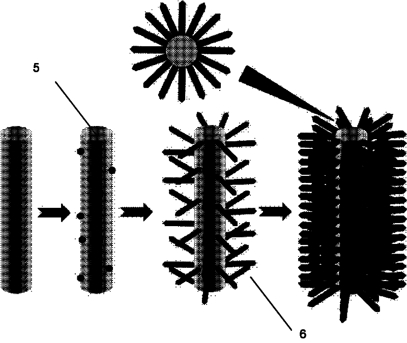
[0054] In a 50ml Erlenmeyer flask, add 0.45g polyvinylpyrrolidone (PVP) into 7.5ml ethanol, stir at room temperature for 8h until the solution is completely clear.

[0055] Take another 10ml Erlenmeyer flask, add 1.5g butyl titanate, 3ml ethanol and 3ml acetic acid in sequence, stir vigorously at room temperature for 10min until completely dissolved. The polymer solution was mixed with the metal salt solution and stirred at room temperature for 1 hour.

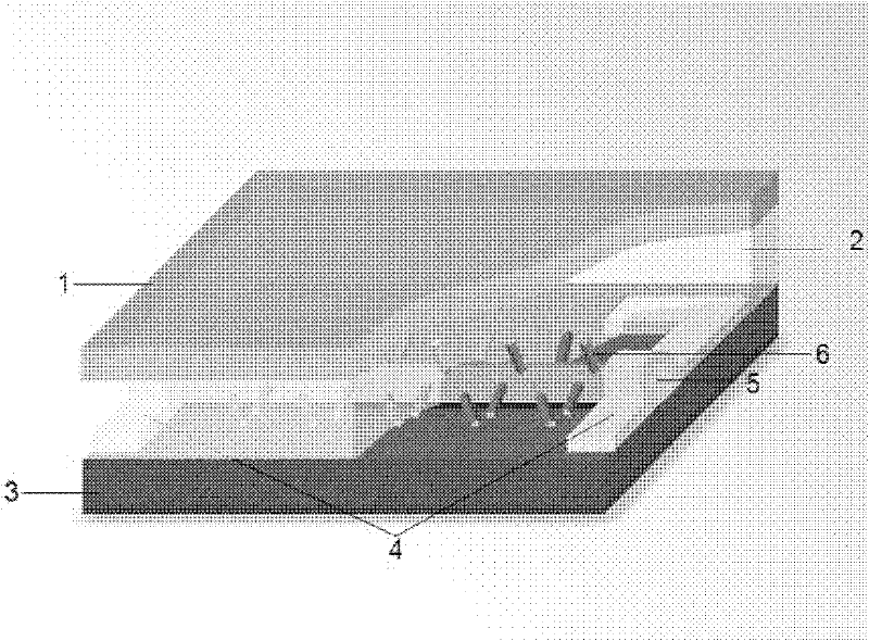
[0056]Put the mixed solution into the spinneret of the electrospinning equipment, the inner diameter of the spinneret head is 1mm, the aluminum sleeve is used as the anode, and the parallel aluminum strips (distance 2.2cm) are used as the cathode to accept the product, and the distance between the two poles is 20 cm, and an applied voltage of 10 kV was used for electrospinning. In this way, parallel arrangement of polyvinylpyrrolidone-containing nanofibers will be obtained between the two parallel aluminum strips of the catho...

Embodiment 2

[0063] Solution preparation and spinning process are consistent with Example 1.

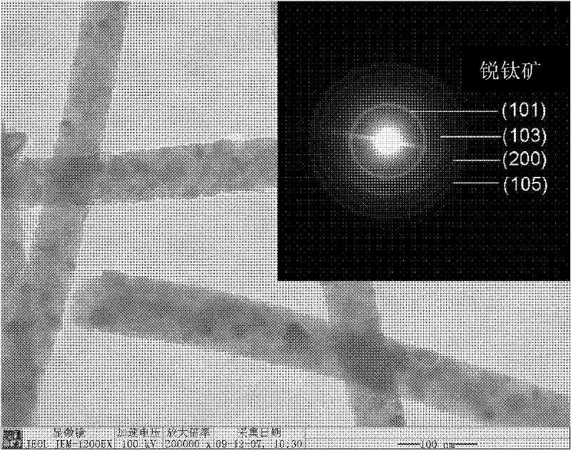
[0064] The quartz wafer substrate was ultrasonically cleaned in ethanol, acetone and deionized water in order to collect the aligned fibers between the two aluminum strips, placed in the air for 12 hours, then placed in a muffle furnace, and slowly heated to 450°C for sintering at a constant temperature for 5 The macromolecule PVP was completely removed within hours, and titanium dioxide nanofibers were obtained. Take a 50ml beaker, add 15ml of water, 15ml of concentrated hydrochloric acid and 0.5g of butyl titanate in sequence, stir evenly until the solution is clear, transfer it together with the quartz sheet attached with parallel anatase titanium dioxide nanofibers to a 40ml hydrothermal reaction kettle, Place in a constant temperature oven at 150°C for 3 hours, take out the quartz slices, wash and dry them. The rutile nanorods on the fiber surface are significantly shorter and thinner than ...

Embodiment 3

[0067] Solution preparation and spinning process are consistent with Example 1.

[0068] The quartz wafer substrate was ultrasonically cleaned in ethanol, acetone and deionized water in order to collect the aligned fibers between the two aluminum strips, placed in the air for 12 hours, then placed in a muffle furnace, and slowly heated to 450°C for sintering at a constant temperature for 5 The macromolecule PVP was completely removed within hours, and titanium dioxide nanofibers were obtained. Take a 50ml beaker, add 15ml of water, 15ml of concentrated hydrochloric acid and 0.5g of butyl titanate in sequence, stir evenly until the solution is clear, transfer it together with the quartz sheet attached with parallel anatase titanium dioxide nanofibers to a 40ml hydrothermal reaction kettle, Place in a constant temperature oven at 150°C for 2 hours, take out the quartz slices, wash and dry them. The arrangement of rutile nanorods on the fiber surface is sparser, obviously shorte...


PUM

PropertyMeasurementUnit
thicknessaaaaaaaaaa
electrical resistivityaaaaaaaaaa
thicknessaaaaaaaaaa

Abstract

The invention relates to the technical field of semiconductor micro-electronic parts, and in particular relates to nanometer semiconductor materials with a multilevel heterostructure manufactured by combining an electrospinning technology with a hydrothermal synthesis technology and a method for manufacturing a micro-electronic part with stable performances by using the nanometer semiconductor materials. In the method, inorganic oxide nanofibers obtained by adopting the electrospinning technology to sinter is takend as a core. The method comprises the following steps: depositing and growing inorganic oxide nanorods on fiber surfaces sequentially by the hydrothermal reaction to obtain single-dimensional arborescent nanometer materials with the multilevel heterostructure; and assembling an FET (field-effect transistor). The FET has higher electron mobility and exceeds the vast majority of FETs in the long service life and the high stability. The maximum electron mobility of anatase titanium dioxide nanofiber/ titanic schorl titanium dioxide nanorod FETs with the multilevel heterostructure can be above 10cm<2>/Vs, and the performances do not attenuate hardly with the increment of thetime and the humidity.

Description

technical field [0001] The invention belongs to the technical field of nano-semiconductor microelectronic devices, and specifically relates to a method for preparing a nano-semiconductor material with a multi-level heterogeneous structure by using an electrospinning technology combined with a hydrothermal synthesis technology, and is used to construct a high-performance and stable microelectronic device. Background technique [0002] Due to the advantages of small size, light weight, high reliability, fast working speed, and high read and write density, microelectronic devices have a huge impact on the development of the information age. Field-effect transistor is the simplest and most important structural unit in current semiconductor electronic devices, and it is the most deeply researched device at present. According to the type of material, it can be divided into non-field effect transistors and organic field effect transistors. Although organic field effect transistors ...

Claims


Application Information

Patent Timeline
Patent Type & Authority Applications(China)
IPC IPC(8): H01L21/04H01L21/34C03C17/00D01F9/10D06M11/36
Inventor 王策王兆杰李振宇张弘楠王威徐秀茹姜婷婷
Owner JILIN UNIV
Why Eureka
Try Eureka