Molecular biosensor and method of single-molecule detection of DNA or protein using the same
A technology of biosensors and devices, applied in the direction of electrochemical variables of materials, etc., can solve the problems of difficult real-time detection, high sensitivity, selectivity, and lack of
- Summary
- Abstract
- Description
- Claims
- Application Information
AI Technical Summary
Problems solved by technology
Method used
Image
Examples
Embodiment 1
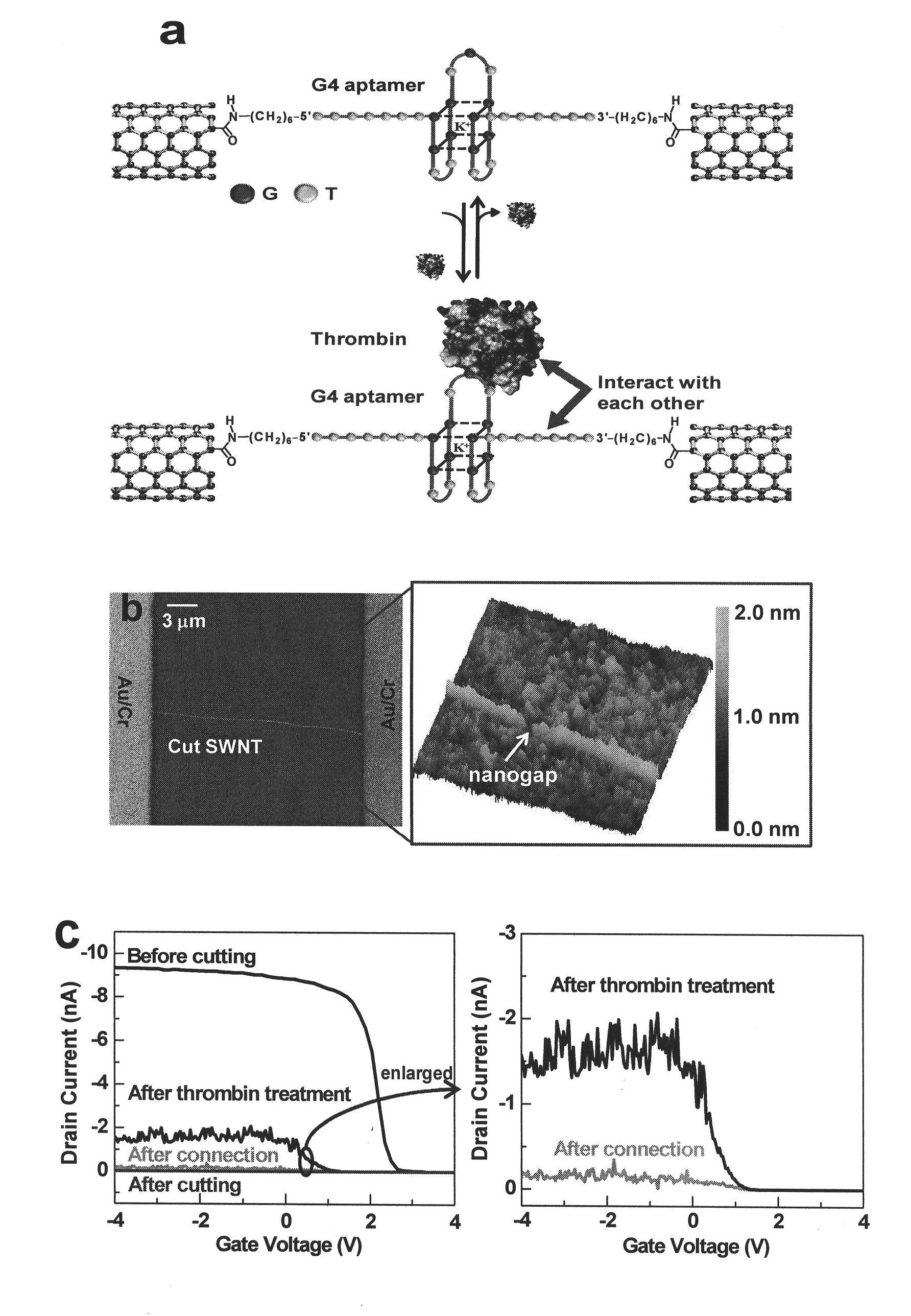
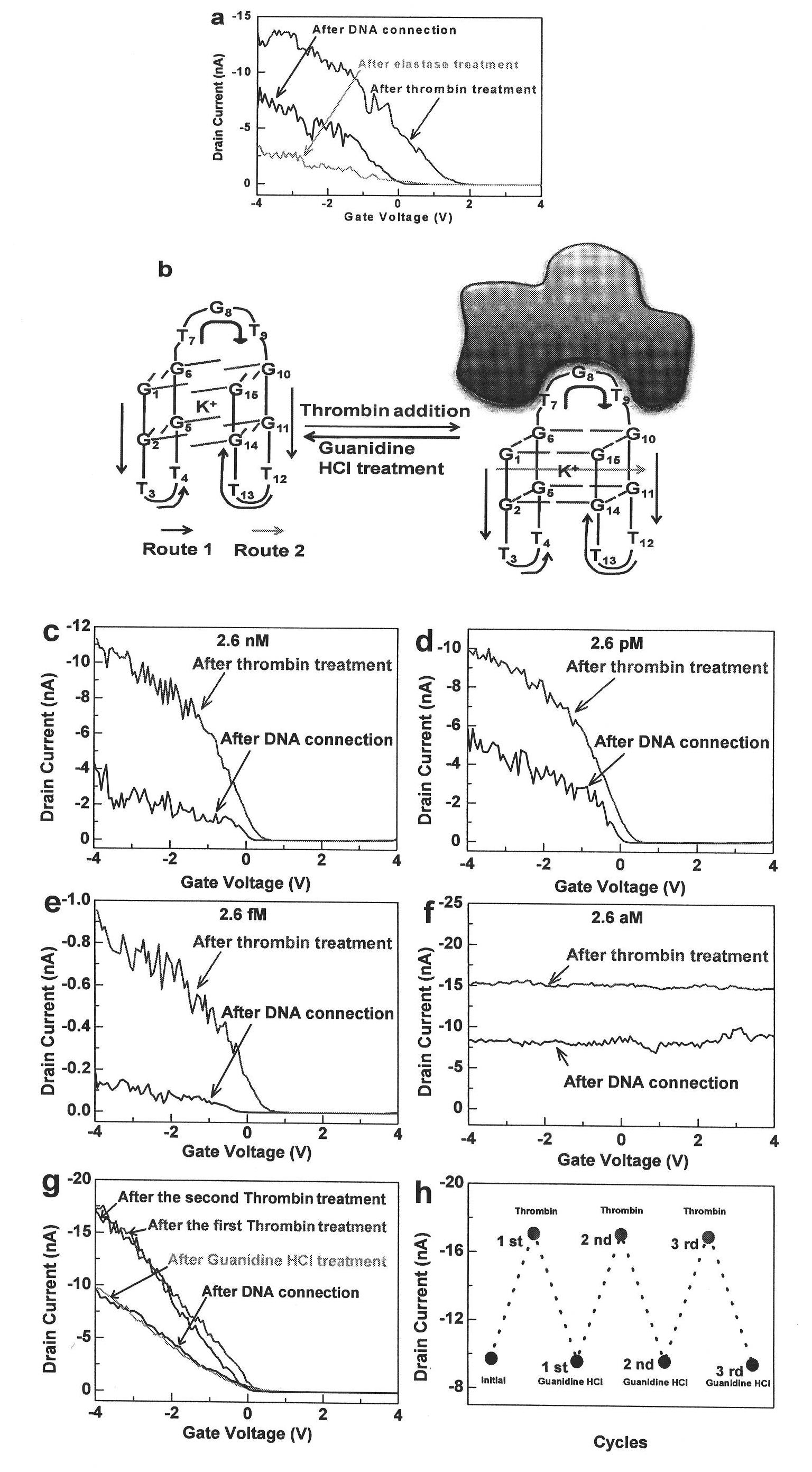
[0049] Example 1: Application of single-molecule aptamer device to detect Thrombin
[0050] 1. Preparation of single-molecule aptamer devices
[0051] 1) On a highly conductive silicon chip substrate containing a thermal oxide layer of silicon dioxide with a thickness of 300nm (resistivity 5-20ohm cm -1 ), use chemical vapor deposition to grow high-quality ultra-long carbon nanotube arrays, and sequentially vapor-deposit Cr (5nm) and Au (50nm) on a single-walled carbon nanotube (7000 μm in length) at an interval of about 20 microns. As the source and drain of the device, construct the SWNT transistor device;
[0052] 2) The SWNT device obtained in step 1) is subjected to ultra-fine electron beam etching and oxidation cutting, and a nano-gap of 1-10 nm is obtained between the carbon tubes, figure 1 Figure b in the middle shows the SEM and AFM pictures of the device. The diameter of the carbon tube in the figure is ~1.2nm, and the size of the nanogap is ~10nm;
[0053] 3) In...
Embodiment 2
[0073] Example 2, the application of single-molecule aptamer device to detect immunoglobulin E (IgE)
[0074] Immunoglobulin E is a class of allotropic antibodies with a δ chain, and is the main antibody involved in the regulation of the pathogenesis of allergic rhinitis, allergic asthma, and eczema. The detection of IgE is of great significance to the study of allergic diseases.
[0075] 1. Preparation of single-molecule aptamer devices
[0076] 1) On a highly conductive silicon chip substrate containing a thermal oxide layer of silicon dioxide with a thickness of 300nm, use chemical vapor deposition to grow high-quality ultra-long carbon nanotube arrays, in a single-walled carbon nanotube (length Cr (5nm) and Au (50nm) were successively vapor-deposited at intervals of about 20 microns (7000 microns) as the source and drain of the device to construct a SWNT transistor device;
[0077] 2) The SWNT device obtained in step 1) is subjected to ultra-fine electron beam etching an...
Embodiment 3
[0087] Example 3, Application of single-molecule aptamer device to detect vascular endothelial growth factor (VEGF)
[0088] Vascular endothelial growth factor is a specific heparin-binding growth factor for vascular endothelial cells, which can induce angiogenesis in vivo and directly affect the content of VEGF in the process of tumor growth and spread. The detection of VEGF can be applied to the diagnosis and treatment of cancer.
[0089] 1. Preparation of single-molecule aptamer devices
[0090] 1) On a highly conductive silicon chip substrate containing a thermal oxide layer of silicon dioxide with a thickness of 300nm, use chemical vapor deposition to grow an array of high-quality ultra-long carbon nanotubes, in a single-walled carbon nanotube ( Cr (5nm) and Au (50nm) were successively vapor-deposited at intervals of about 20 microns on the length of 7000 microns as the source and drain of the device to construct a SWNT transistor device;
[0091] 2) The SWNT device obta...
PUM
| Property | Measurement | Unit |
|---|---|---|
| Length | aaaaa | aaaaa |
| Thickness | aaaaa | aaaaa |
| Thickness | aaaaa | aaaaa |
Abstract
Description
Claims
Application Information


