Method for preparing active layer structure with high-density gallium nitride quantum dots

A gallium nitride quantum, high-density technology, applied in phonon exciters, laser parts, semiconductor lasers, etc., can solve the problems of large size, poor uniformity of quantum dot size distribution, and inability to improve the surface density of quantum dots.

Active Publication Date: 2012-04-18
NANJING UNIV
View PDF7 Cites 17 Cited by
  • Summary
  • Abstract
  • Description
  • Claims
  • Application Information

AI Technical Summary

Problems solved by technology

Due to the large lattice mismatch between III-nitride semiconductors, the size of GaN or InGaN quantum dots obtained in S-K growth mode is relatively large (>50nm), so that the surface density of quantum dots cannot be increased.
Secondly, the uniformity of the size distribution of quantum dots is poor, which leads to the deviation of the energy statistical distribution of the density of states of quantum dots, which is not conducive to improving the efficiency of LEDs an

Method used


Image

  • Method for preparing active layer structure with high-density gallium nitride quantum dots
  • Method for preparing active layer structure with high-density gallium nitride quantum dots
  • Method for preparing active layer structure with high-density gallium nitride quantum dots

Examples


Embodiment Construction

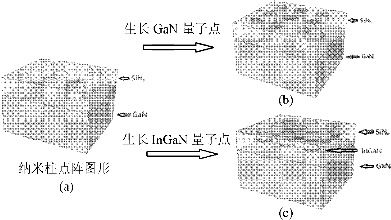
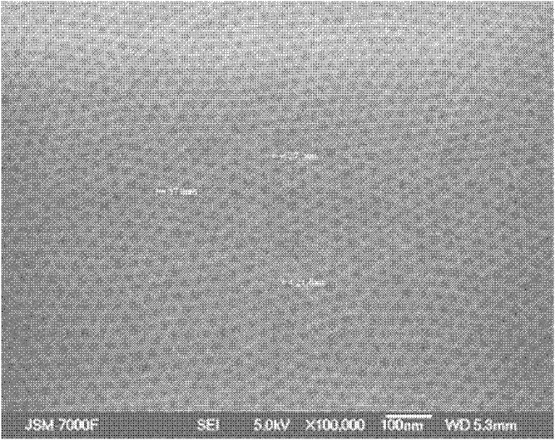
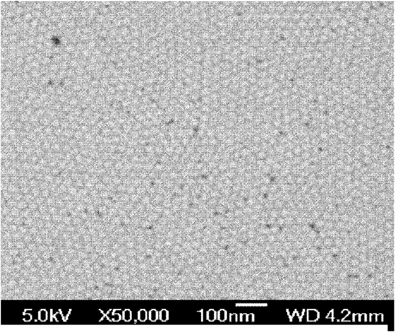
[0018] The invention uses a low-cost block copolymer photolithography technology to prepare nano-column lattice patterns on GaN templates, and the process is divided into two parts: preparation of nano-column lattice patterns and secondary epitaxial growth of GaN-based quantum dots.

[0019] The specific implementation plan for the preparation of the nano-column lattice pattern is as follows: first, a layer of dielectric film is deposited on the GaN film by PECVD method, and the first scheme of this embodiment uses SiN x . PECVD-grown SiN x Thin film adopts standard process, in order to obtain high quality SiN x film, we use NH-free 3 Source SiN x grow. Silane (SiH 4 ) and nitrogen (N 2 ) gas source, the reaction source generates a chemically active plasma under the ionization of radio frequency (RF), through the chemical reaction SiH x +N→SiN x (+H 2 ) to deposit SiN on a GaN template heated to 300°C x Thin film mask layer, typically SiN x The thickness is 10-50nm....


PUM

PropertyMeasurementUnit
Thicknessaaaaaaaaaa
Diameteraaaaaaaaaa
Depthaaaaaaaaaa

Abstract

The invention relates to a method for preparing an active layer structure with high-density gallium nitride quantum dots; the method comprises the following steps of: (1). depositing a layer of SiO or SiNx dielectric thin film material with the thickness of 10-50nm on a GaN template or surfaces of other semiconductor films, painting a mixing copolymer of PS (Polystyrene) and PMMA (Polymenthyl Methacrylate) on the surface of the dielectric thin film, obtaining a PS nanometer column graph after cleaning the PMMA, transferring the PS nanometer column graph to the dielectric thin film layer by adopting plasma etching, wherein the PS nanometer column graph is prepared according to the following parameters: (1) the surface density reaches 0.8-1.0*1011cm<-2>; (2) the PS nanometer column graph istransferred to the SiNx or SiO2 dielectric thin film layer by adopting reactive ion etching, the PP is removed to obtain a template on which a GaN nanometer point structure grows for the second time through MOCVD (Metal-organic Chemical Vapor Deposition); and (3) a GaN-base quantum dot structure grows, emits strong royal purple light and is used for manufacturing the active layer structure in a light-emitting diode (LED) with high efficiency and a laser device (LD) optoelectronic device.

Description

technical field [0001] The invention relates to a design and preparation method of an active layer structure in a light-emitting diode (LED) and a laser (LD) based on gallium nitride (GaN)-based compound semiconductors, in particular to nitrogen with high density and uniform size distribution in the active layer The invention relates to a preparation method of a gallium nitride quantum dot structure and an indium gallium nitride-gallium nitride quantum dot structure, belonging to the technical field of nanometer science and semiconductor material epitaxial growth. Background technique [0002] Gallium Nitride (GaN) and its alloys Indium Gallium Nitride (InGaN) and Aluminum Gallium Nitride (AlGaN) are the preferred materials for preparing short-wavelength blue-violet light-emitting diodes (LEDs) and lasers (LDs) optoelectronic devices. LED and LD are the core light-emitting components of the new all-solid-state semiconductor lighting source. Compared with traditional lighting...

Claims


Application Information

Patent Timeline
IPC IPC(8): H01L33/06H01S5/343
Inventor 刘斌张荣李烨操谢自力方贺男庄喆陈鹏修向前赵红陈敦军顾书林韩平郑有炓托马斯·科奇
Owner NANJING UNIV
Why Eureka
Try Eureka