Annular semiconductor laser of vertical coupling structure and preparing method thereof

A ring laser and vertical coupling technology, which is applied in the direction of semiconductor lasers, lasers, laser components, etc., can solve the problems of increasing the difficulty and complexity of process preparation, poor reliability and stability of devices, etc., and achieve low loss, stable device performance, The effect of simple process

Inactive Publication Date: 2013-08-21
TIANJIN UNIV
View PDF2 Cites 23 Cited by
  • Summary
  • Abstract
  • Description
  • Claims
  • Application Information

AI Technical Summary

Problems solved by technology

[0004] The existing vertical coupling structure uses molecular beam epitaxy (MBE) or metal organic compound chemical vapor deposition (MOCVD) secondary growth technology to grow the material structure of ring resonator and strip waveguide respectively. This secondary growth technology with pattern , increasing the difficulty and complexity of process preparation
In addition, there are also vertically coupled ring lasers that use a bonding process to realize a microring resonator and a strip waveguide, but the reliability and stability of the device are relatively poor

Method used


Image

  • Annular semiconductor laser of vertical coupling structure and preparing method thereof
  • Annular semiconductor laser of vertical coupling structure and preparing method thereof
  • Annular semiconductor laser of vertical coupling structure and preparing method thereof

Examples


Embodiment 1

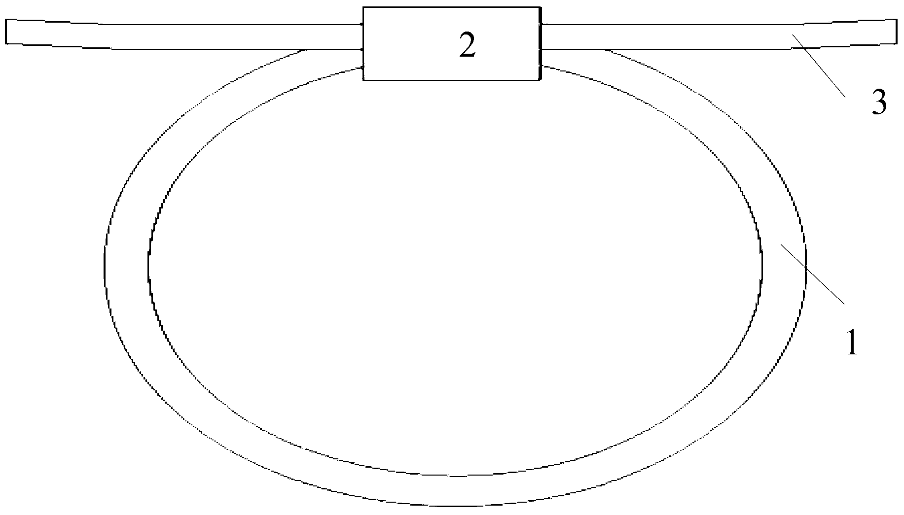
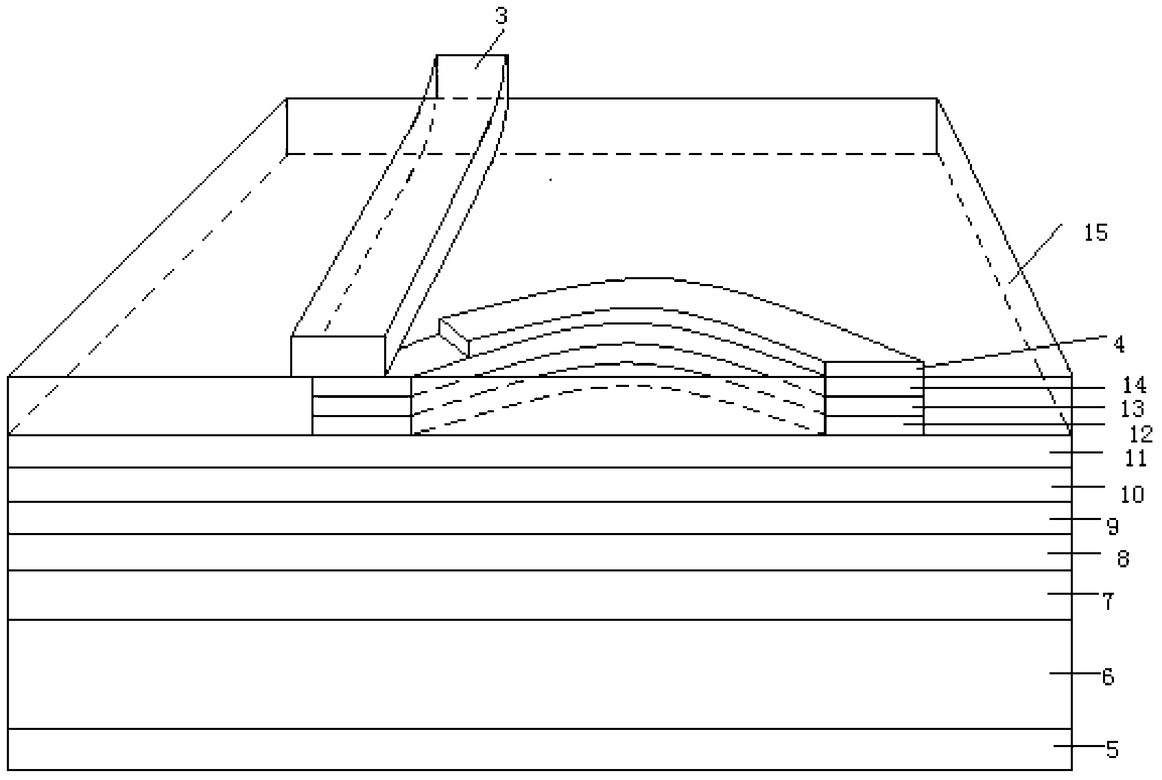
[0050] see figure 2 and image 3 , the preparation process of InP-based semiconductor ring laser is as follows:

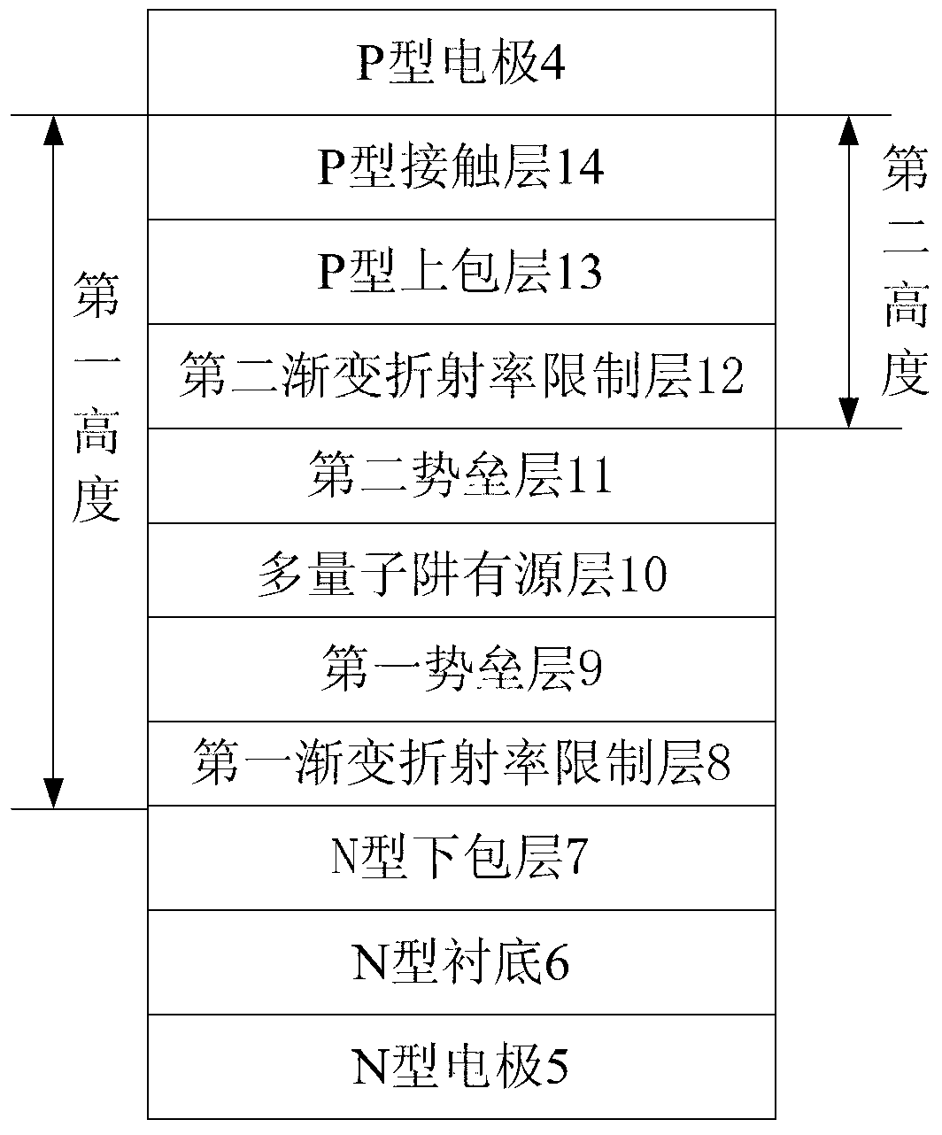
[0051] 1. On the N-type InP substrate 6 with (100) crystal orientation, use metal-organic chemical vapor deposition or molecular beam epitaxy to grow a thickness of 1000-2000nm and a doping concentration of 1×10 18 cm -3The N-type InP lower cladding layer 7; the InP lower cladding layer 7 also serves as a buffer layer for epitaxial growth, so as to reduce the defect density of the epitaxial growth thin layer thereon.

[0052] 2. Sequentially grow the first graded-index confinement layer 8, the first barrier layer 9, the AlGaInAs multi-quantum well active layer 10, the second barrier layer 11, and the second graded-refraction confinement layer 12 of AlGaInAs quaternary system material ;

[0053] Wherein, the thickness of the first graded index confining layer 8 is 50 nm, and the doping concentration is 1×10 18 cm -3 The thickness of the first barrier layer 9 ...

Embodiment 2

[0070] see figure 2 and image 3 , the fabrication process of GaAs-based semiconductor ring laser is as follows:

[0071] 1. On an N-type GaAs substrate 6 with a (100) crystal orientation, grow it with a thickness of 1000-2000 nm and a doping concentration of 1×10 by metal-organic chemical vapor deposition or molecular beam epitaxy. 18 cm -3 The N-type AlGaAs lower cladding layer 7; the AlGaAs lower cladding layer 7 also serves as a buffer layer for epitaxial growth, so as to reduce the defect density of the epitaxial growth thin layer thereon.

[0072] 2. Sequentially grow the first graded index confinement layer 8, the first barrier layer 9, the AlGaAs multi-quantum well active layer 10, the second barrier layer 11 and the second graded index confinement layer 12 of AlGaAs ternary system material ;

[0073] Wherein, the thickness of the first graded index confining layer 8 is 50 nm, and the doping concentration is 1×10 18 cm -3 The thickness of the first barrier layer...


PUM


Abstract

The invention discloses an annular semiconductor laser of a vertical coupling structure and a preparing method thereof. An annular active resonator cavity is any one closed loop composed of ridge type waveguide and strip type waveguide, a P type electrode and an N type electrode are arranged on the annular active resonator cavity, laser light in the annular active resonator cavity is coupled to strip type straight waveguide through a vertical coupler, and the strip type straight waveguide outputs the laser light. An N type lower wrapping layer, a first gradual-change refractive index limiting layer, a first barrier layer, a multiple quantum well active layer, a second barrier layer, a second gradual-change refractive index limiting layer, a P type upper wrapping layer and a P type contacting layer which have preset thicknesses and concentration are successively formed by means of a metal organism chemical vapor deposition or molecular beam epitaxy method. A plurality of epitaxial layers are etched by using a SiO2 image as a mask, the etching depth is less than or equal to a first height and greater than or equal to a second height, and the annular active resonator cavity is transferred to a chip. The obtained annular semiconductor laser has the advantages of being simple in process, low in cost, stable in performance of parts, high in reliability and the like.

Description

technical field [0001] The invention relates to the field of semiconductor lasers, in particular to a semiconductor ring laser with a vertical coupling structure and a preparation method thereof. Background technique [0002] The semiconductor ring laser uses a closed waveguide loop as a resonant cavity, does not need a cleavage surface or a grating to provide optical feedback, and can be deflected arbitrarily with the crystal direction. It has a compact structure, simple process, high reliability, and is fully compatible with existing microelectronics processes. Achieve high-density integration. It can not only realize tunable light source, optical switch, wavelength conversion and other functions, but also can construct key devices and components in optical networks such as all-optical logic and optical random access memory, and solve the compatibility of device structure and manufacturing process in monolithic optoelectronic integrated circuits. sexual issues. Therefore...

Claims


Application Information

Patent Timeline
Patent Type & Authority Applications(China)
IPC IPC(8): H01S5/10H01S5/22H01S5/026
Inventor 谢生郭婧毛陆虹张世林郭维廉
Owner TIANJIN UNIV
Why Eureka
Try Eureka