Preparation method of large-area single-layer or multi-layer molybdenum diselenide single chip

A molybdenum diselenide, large-area technology, applied in chemical instruments and methods, single crystal growth, single crystal growth, etc., can solve the problems of uneven MoSe2 morphology, inapplicability to large-scale production and application, and difficult control of thickness , to achieve the effect of high crystallinity, high repeatability and short synthesis cycle

Inactive Publication Date: 2014-03-05
TECHNICAL INST OF PHYSICS & CHEMISTRY - CHINESE ACAD OF SCI
View PDF2 Cites 18 Cited by
  • Summary
  • Abstract
  • Description
  • Claims
  • Application Information

AI Technical Summary

Problems solved by technology

However, these preparation methods have their own shortcomings, such as physical exfoliation, although high-quality single-layer or several molecular layers of MoSe can be obtained. 2 , but the repeatability of this method is poor, and the prepared MoSe 2 The area is relatively small, not suitable for large-scale production and application; MoSe obtained by hydrothermal synthesis 2 The morphology is not uniform and the crystallinity is poor, and high temperature treatment is required to improve its crystallinity; and the use of metal molybdenum high temperature selenization method can obtain a large area of ​​MoSe 2 , but its thickness is difficult to control, and the prepared MoSe 2 The thin film is also mostly polycrystalline

Method used


Image

  • Preparation method of large-area single-layer or multi-layer molybdenum diselenide single chip
  • Preparation method of large-area single-layer or multi-layer molybdenum diselenide single chip
  • Preparation method of large-area single-layer or multi-layer molybdenum diselenide single chip

Examples


Embodiment 1

[0035] ⑴ Cleaning of silicon dioxide / silicon substrate:

[0036] ① Cut 1cm*2cm SiO2 with a glass knife 2 / Si substrate.

[0037] ② In a fume hood, firstly clean the substrate ultrasonically with acetone for 5 minutes, then ultrasonically clean it with absolute ethanol for 5 minutes, and finally rinse it with deionized water.

[0038] ③Then put the substrate into a mixture of concentrated sulfuric acid and hydrogen peroxide (3:1) and boil for 10 minutes.

[0039] ④ Rinse the substrate with deionization and dry it with nitrogen.

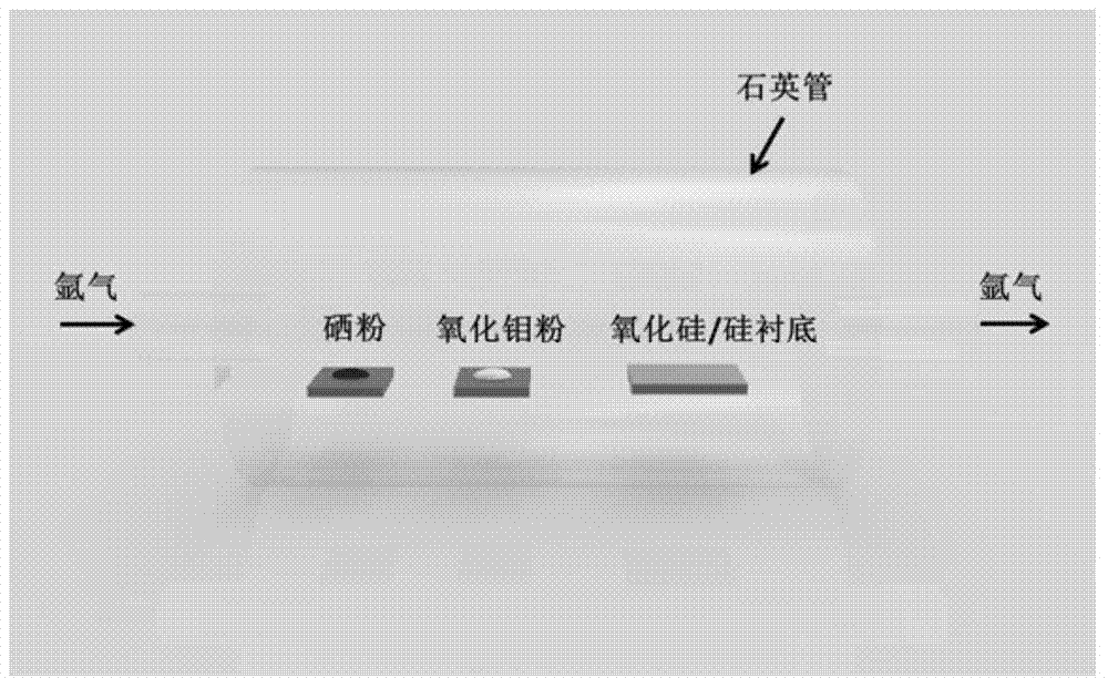
[0040] ⑵ SiO 2 The / Si substrate was placed 1 cm downstream from the center of the high temperature zone of the tube furnace. Weigh 20mg of MoO 3 The powder (not less than 99.90% purity) is placed in a ceramic boat, which is then placed in the center of the high temperature zone of the tube furnace. 0.8 g of Se powder was weighed into a ceramic boat, which was then placed 6 cm upstream of the high temperature zone of the tube furnace.

[0041] (...

Embodiment 2

[0045] ⑴ Cleaning of silicon dioxide / silicon substrate:

[0046] ① Cut 1cm*2cm SiO2 with a glass knife 2 / Si substrate.

[0047] ② In a fume hood, firstly clean the substrate ultrasonically with acetone for 5 minutes, then ultrasonically clean it with absolute ethanol for 5 minutes, and finally rinse it with deionized water.

[0048] ③ Then put the substrate into a mixture of concentrated sulfuric acid and hydrogen peroxide (3:1) and boil for 10 minutes.

[0049] ④ Rinse the substrate with deionization and dry it with nitrogen.

[0050] ⑵ SiO 2 The / Si substrate is placed 1 cm downstream of the center of the high temperature zone of the tube furnace. Weigh 10mg of MoO 3 The powder (not less than 99.90% purity) is placed in a ceramic boat, which is then placed in the center of the high temperature zone of the tube furnace. 0.5 g of Se powder was weighed into a ceramic boat, which was then placed 6 cm upstream of the high temperature zone of the tube furnace.

[0051] (3)...

Embodiment 3

[0055] ⑴ Cleaning of silicon dioxide / silicon substrate:

[0056] ① Cut 1cm*2cm SiO2 with a glass knife 2 / Si substrate.

[0057] ② In a fume hood, firstly clean the substrate ultrasonically with acetone for 5 minutes, then ultrasonically clean it with absolute ethanol for 5 minutes, and finally rinse it with deionized water.

[0058] ③Then put the substrate into a mixture of concentrated sulfuric acid and hydrogen peroxide (3:1) and boil for 10 minutes.

[0059] ④ Rinse the substrate with deionization and dry it with nitrogen.

[0060] ⑵ SiO 2 / Si substrate is placed downstream of the center of the high temperature zone of the tube furnace, 1cm away from the center of the high temperature zone, and 10mg of MoO is weighed 3 The powder (not less than 99.90% purity) is placed in a ceramic boat, which is then placed in the center of the high temperature zone of the tube furnace. Weigh 0.5g of Se powder and place it in a ceramic boat, and then place it at the upstream of the h...


PUM


Abstract

The invention discloses a preparation method of a large-area single-layer or multi-layer molybdenum diselenide single chip. The method comprises the following steps: 1) cleaning a substrate; (2) putting the substrate, molybdenum trioxide powder and selenium powder into a reaction furnace; 3) vacuumizing the interior of the reaction furnace, and introducing an inactive gas; 4) warming, reacting and naturally cooling inside the reaction furnace, and taking out the substrate, so as to obtain a large-area reaction product on the substrate. The method is simple in operation, high in repeatability and strong in controllability; the prepared MoSe2 has the advantages of being large in area, good in uniformity, high in quality and the like, and has important research value and broad application prospect in the fields of solar cells, field effect transistors, photocatalytic hydrogen generation and the like.

Description

technical field [0001] The invention relates to the field of nano-semiconductor technology, in particular to a method for preparing a large-area single-layer or several-layer molybdenum diselenide single wafer. Background technique [0002] Graphene has excellent optical, electrical, mechanical, and thermal properties, and has great potential application value in the fields of electronic information, communication technology, biology, catalysis, and sensing. It has become one of the most concerned two-dimensional nanomaterials today. one. In 2004, physicist Andre Geim of the University of Manchester and his student Konstantin Novoselov successfully exfoliated graphene from graphite with ordinary tape , thereby overturning the theory that graphene cannot exist alone. However, the bandgap width (Eg) of graphene is 0eV, which greatly limits the application of graphene in the fields of semiconductor electronics and optoelectronics. For this reason, people turn their attention...

Claims


Application Information

Patent Timeline
Patent Type & Authority Applications(China)
IPC IPC(8): C30B29/46C30B1/10C30B29/64
Inventor 孟祥敏夏静黄兴
Owner TECHNICAL INST OF PHYSICS & CHEMISTRY - CHINESE ACAD OF SCI
Why Eureka
Try Eureka