Method for preparing high-adhesion micro-nano array structure film through wet etching and reverse transfer printing

A technology with an array structure and high adhesion, applied in the field of nanomaterials, can solve the problems of expensive optical exposure equipment, harsh processing environment, complex process flow, etc., to achieve simple and fast operation, simple solution ratio, and strong adjustability Effect

Inactive Publication Date: 2014-09-17
HEFEI INSTITUTES OF PHYSICAL SCIENCE - CHINESE ACAD OF SCI
View PDF10 Cites 23 Cited by
  • Summary
  • Abstract
  • Description
  • Claims
  • Application Information

AI Technical Summary

Problems solved by technology

However, the above methods for preparing micro-nano adhesive structure arrays require either expensive ion etching and optical exposure equipment, harsh processing environments, or complex process flows, and there are disadvantages such as instrument maintenance.
At present, there is no report in the literature on the preparation of a high-adhesion array structure film using a wet etching method to prepare a template silicon wafer and a micro-nano structure transfer technology.

Method used


Image

  • Method for preparing high-adhesion micro-nano array structure film through wet etching and reverse transfer printing
  • Method for preparing high-adhesion micro-nano array structure film through wet etching and reverse transfer printing
  • Method for preparing high-adhesion micro-nano array structure film through wet etching and reverse transfer printing

Examples


Embodiment

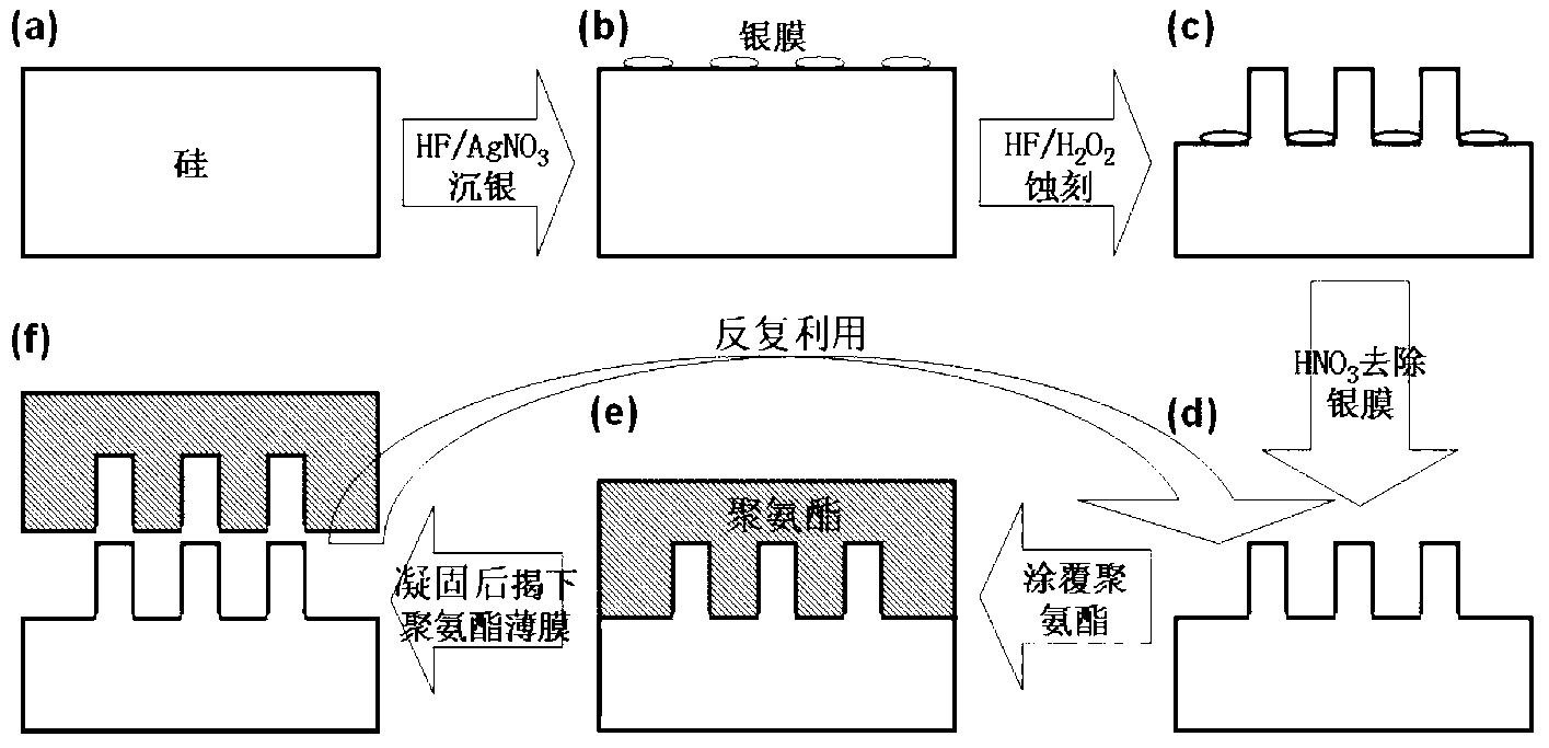
[0025] Taking the preparation of highly adhesive nanowire array structure film as an example

[0026] (1) Silicon wafer cleaning: use alcohol, acetone, hydrogen peroxide (mass fraction 30%): ammonia water (mass fraction 25%-28%): deionized water = 1:1:5 (volume ratio) to ultrasonically clean the single crystal Silicon wafers for 20 minutes, then soaked in hydrogen peroxide (30% mass fraction): concentrated sulfuric acid (98% mass fraction): deionized water = 3:1 (volume ratio) for 8 hours;

[0027] (2) Deposit porous silver film on silicon wafer: 0.5mmol (0.085g) silver nitrate (AgNO 3 ) and 0.46mol (20ml) hydrofluoric acid (HF, 40% mass fraction) diluted to 100ml, after stirring evenly, put the silicon wafer cleaned in step (1) into it, and let it stand at room temperature 25°C to deposit silver film for 2 minutes to obtain a silicon wafer with a porous silver film grown on the surface;

[0028] (3) Silicon nanowire array structure of required length "growth" on the silicon...


PUM


Abstract

The invention discloses a method for preparing a high-adhesion micro-nano array structure film through wet etching and reverse transfer printing. The method comprises the following steps: with a silver nitrate/hydrofluoric acid solution as a silver deposition solution, depositing a layer of porous silver film on a silicon chip so as to obtain an etching catalytic metal and etching a desired micro-nano array structure in a hydrofluoric acid/hydrogen peroxide solution or potassium hydroxide/isopropanol solution; carrying out soaking with concentrated nitric acid so as to remove the silver film, carrying out air drying and using the treated silicon chip as a template silicon chip; uniformly coating the template silicon chip with organic matter colloid and standing the template silicon chip for a period of time; and placing the template silicon chip on a heating plate after precipitation and uniform distribution of bubbles, heating the template silicon chip at a certain temperature for a period of time, stripping off a colloid film when the colloid completely solidifies and printing a reversed structure of the prepared micro-nano array structure on the colloid film through transfer printing so as to realize preparation of the high-adhesion micro-nano array structure film. The method is simple to operate, has low cost, is not restricted by a preparation area and can be extensively applied to the field of bionic adhesion.

Description

technical field [0001] The invention relates to a method for preparing a high-adhesive micro-nano array structure film by using a wet etching method and a reverse printing method, and belongs to the technical field of nanometer materials. the Background technique [0002] The reasons for the adhesion of objects are: suction caused by atmospheric pressure, friction, micro-connection (micro-connection usually exists on the surface of adhesives and non-smooth objects), electrostatic attraction, viscose effect (generally refers to animal glands The secreted liquid has a certain viscosity), capillary force, etc. The adhesion principle of the micro-nano adhesion array structure prepared by this method is that the van der Waals force generated between the micro- and nano-scale protrusions on the surface of the polyurethane film and the surface molecules of the object is accumulated (the van der Waals force is A weak electromagnetic attraction produced when neutral molecules are ...

Claims


Application Information

Patent Timeline
Patent Type & Authority Applications(China)
IPC IPC(8): B81C1/00
Inventor 裴志彬吴摞李淑鑫叶长辉
Owner HEFEI INSTITUTES OF PHYSICAL SCIENCE - CHINESE ACAD OF SCI
Why Eureka
Try Eureka