Solar cell device and method for manufacturing same
A solar cell and device technology, applied in the direction of electric solid-state devices, semiconductor/solid-state device manufacturing, electrical components, etc., can solve the problem of low energy conversion efficiency of solar cells
- Summary
- Abstract
- Description
- Claims
- Application Information
AI Technical Summary
Problems solved by technology
Method used
Image

Examples
preparation example Construction
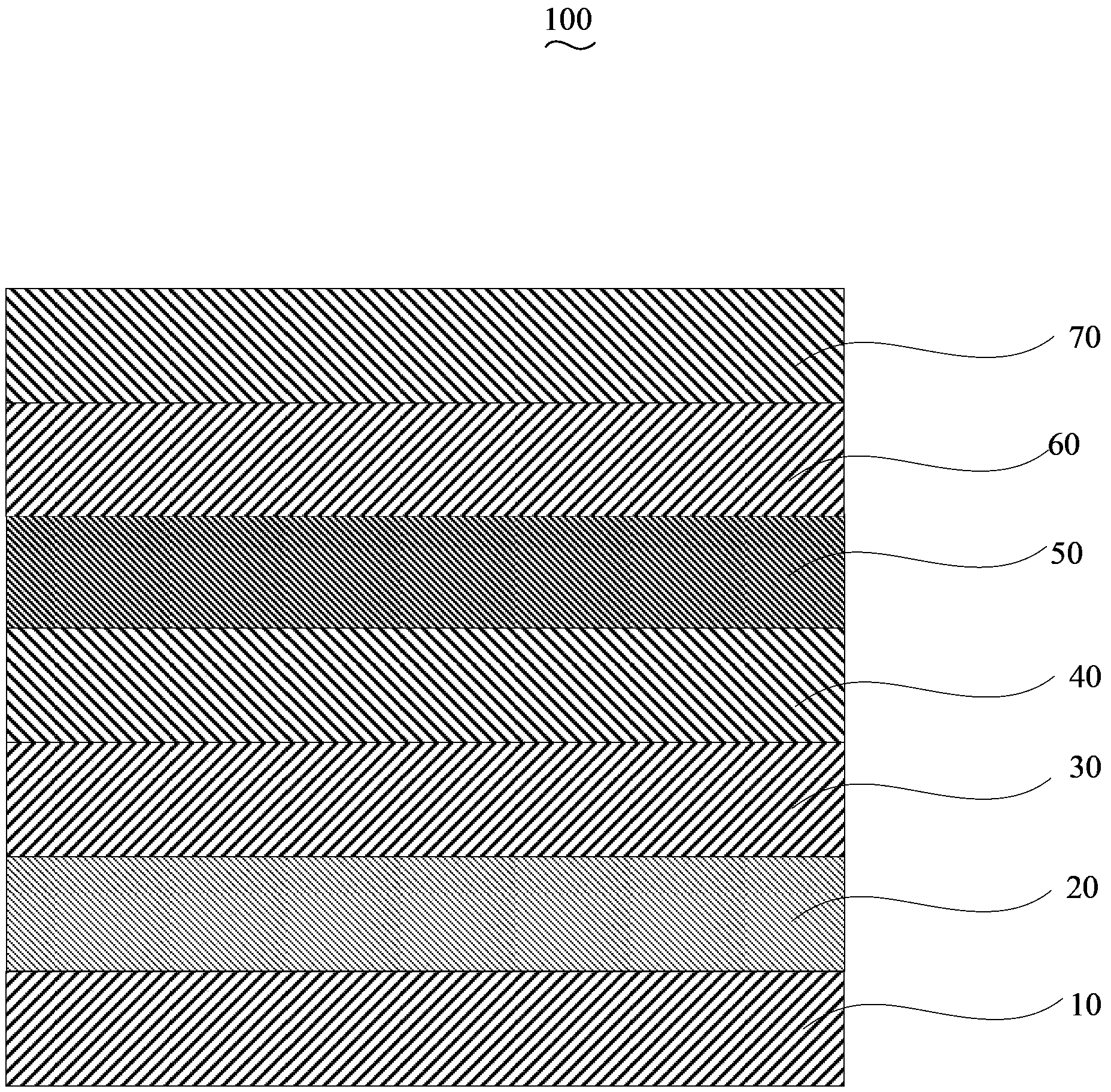
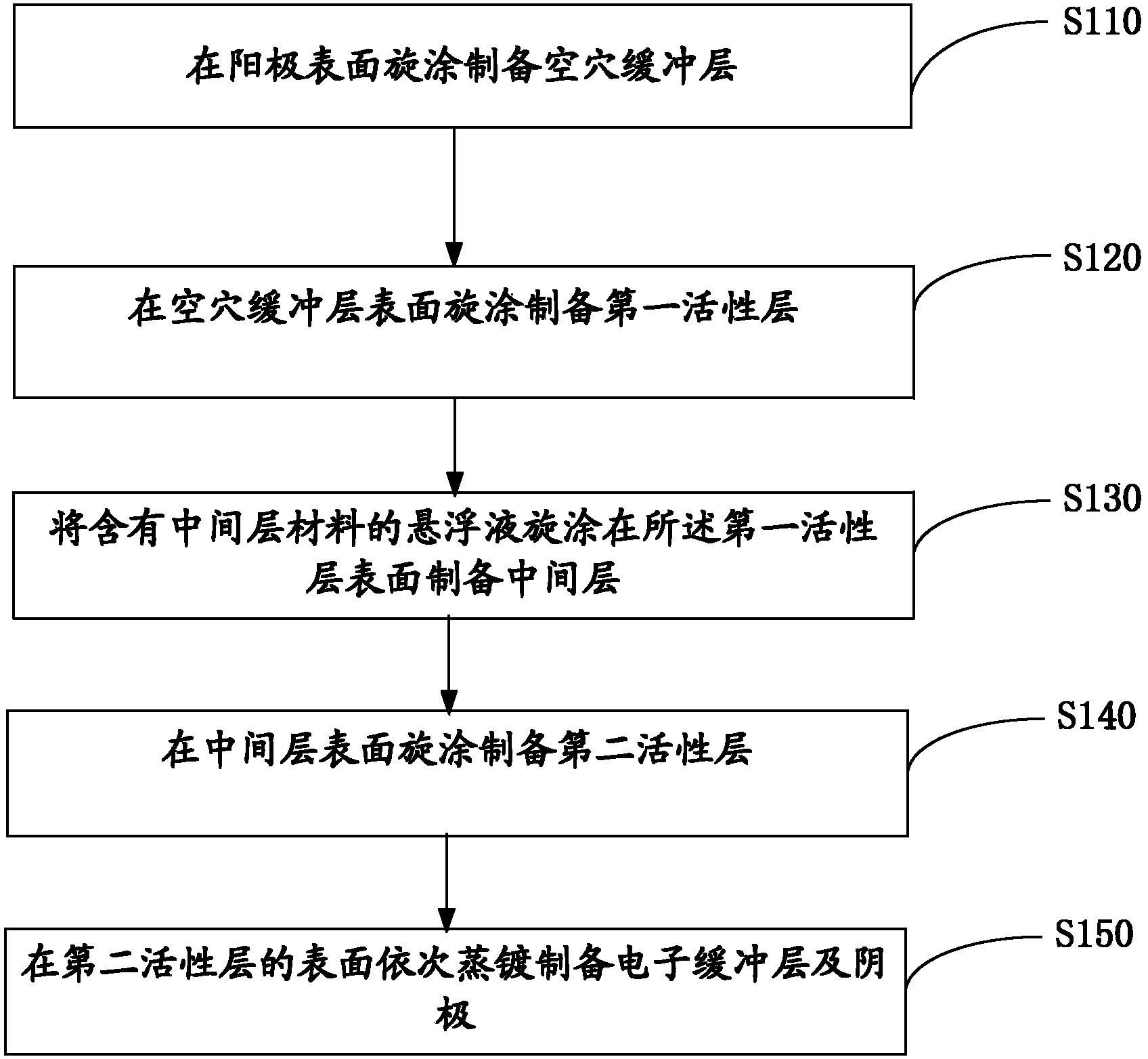
[0034] Please also see figure 2 , the preparation method of the solar cell device 100 of an embodiment, it comprises the following steps:
[0035]Step S110 , preparing a hole buffer layer 20 on the surface of the anode 10 by spin coating.
[0036] The anode 10 is indium tin oxide glass (ITO), fluorine doped tin oxide glass (FTO), aluminum doped zinc oxide glass (AZO) or indium doped zinc oxide glass (IZO).
[0037] In this embodiment, the pretreatment of the anode 10 includes removing organic pollutants on the surface of the anode 10 and performing oxygen ion treatment on the anode 10 . The anode 10 is ultrasonically cleaned with detergent, deionized water, acetone, ethanol, and isopropanone for 15 minutes to remove organic pollutants on the surface of the substrate 10; the anode 10 is treated with oxygen ion for 5 minutes to 15 minutes, and the power is 10 minutes. ~50W.
[0038] The hole buffer layer 20 is prepared by spin-coating a solution containing a hole buffer mate...
Embodiment 1
[0054] The structure prepared in this embodiment is: ITO / PEDOT:PSS / P3HT:PC 61 BM / Bphen:FeCl 3 :P3HT / P3HT:PC 61 BM / LiF / Al solar cell devices. Wherein, " / " indicates a stacked structure, and ":" indicates doping or mixing, and the following embodiments are the same.
[0055] First, carry out photolithography treatment on ITO, cut it into the required size, and then use detergent, deionized water, acetone, ethanol, and isopropanol to sonicate for 15 minutes each to remove organic pollutants on the glass surface; clean the conductive substrate Oxygen plasma treatment was carried out, the treatment time was 10min, and the power was 20W; the hole buffer layer was prepared by spin coating, the material was PEDOT:PSS with a mass ratio of 2:1, the mass fraction of PEDOT was 2%, and the spin coating speed was 4000rpm. The time is 15s, after spin-coating, heat at 200°C for 30min, and the thickness is 70nm; spin-coat the first active layer, the first active layer is composed of P3HT an...
Embodiment 2
[0062] The structure prepared in this example is IZO / PEDOT:PSS / P3HT:PC 61 BM / TAZ:FeBr 3 :P3AT / P3HT:PC 61 BM / Cs 2 CO 3 / Au solar cell devices.
[0063] First, IZO is subjected to photolithography treatment, cut into the required size, and then ultrasonicated with detergent, deionized water, acetone, ethanol, and isopropanol for 15 minutes each to remove organic pollutants on the glass surface; after cleaning, clean the conductive substrate Oxygen plasma treatment was carried out, the treatment time was 15min, and the power was 10W; the hole buffer layer was prepared by spin coating, the material was PEDOT:PSS with a mass ratio of 2:1, the mass fraction of PEDOT was 5%, and the spin coating speed was 6000rpm. The time is 30s, after spin-coating, heat at 100°C for 60min, the thickness is 20nm; spin-coat the first active layer, the first active layer is composed of P3HT and PC with a concentration of 8mg / ml 61 The solution of BM was spin-coated, the solvent was toluene, P3HT ...
PUM
| Property | Measurement | Unit |
|---|---|---|
| Thickness | aaaaa | aaaaa |
| Concentration | aaaaa | aaaaa |
| Thickness | aaaaa | aaaaa |
Abstract
Description
Claims
Application Information
 - R&D
- Intellectual Property
- Life Sciences
- Materials
- Tech Scout
- Unparalleled Data Quality
- Higher Quality Content
- 60% Fewer Hallucinations
Browse by: Latest US Patents, China's latest patents, Technical Efficacy Thesaurus, Application Domain, Technology Topic, Popular Technical Reports.
© 2025 PatSnap. All rights reserved.Legal|Privacy policy|Modern Slavery Act Transparency Statement|Sitemap|About US| Contact US: help@patsnap.com