Preparation method for WS<2>/Si heterojunction solar cell

A solar cell and heterojunction technology, applied in circuits, electrical components, photovoltaic power generation, etc., can solve the problems that cannot be separated from the preparation process of new semiconductor materials, affect the large-scale popularization and application, and the efficiency is close to the theoretical limit. Application prospect, high crystallization performance, low cost effect

Inactive Publication Date: 2016-08-17
HUAZHONG UNIV OF SCI & TECH
View PDF4 Cites 6 Cited by
  • Summary
  • Abstract
  • Description
  • Claims
  • Application Information

AI Technical Summary

Problems solved by technology

At present, although silicon-based solar cells are the most mature in solar cells, their high cost has seriously affected their large-scale application; with the development of technology, the efficiency of today's silicon-based solar cells is close to theoretical It is very difficult to further improve the conversion efficiency; therefore, the development of solar cells is inseparable from the selection of new semiconductor materials and the improvement of the preparation process.

Method used


Image

  • Preparation method for WS&lt;2&gt;/Si heterojunction solar cell
  • Preparation method for WS&lt;2&gt;/Si heterojunction solar cell
  • Preparation method for WS&lt;2&gt;/Si heterojunction solar cell

Examples


preparation example Construction

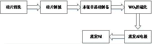
[0030] WS of the present invention 2 / Si heterojunction solar cell preparation method, comprising the following steps:

[0031] (1) Use acetone solution to ultrasonically clean the single crystal silicon wafer to remove organic dirt on the surface of the silicon wafer, and use alcohol to carry out ultrasonic cleaning to the silicon wafer to remove the acetone on the surface of the silicon wafer, and rinse with deionized water for 3 times . Among them, the thickness of monocrystalline silicon wafer is 150 microns to 300 microns, and the resistivity is 0.2Ω•㎝~1.0Ω•㎝.

[0032] (2) Using NH 4 F. Clean the above-mentioned silicon wafer with HF mixed solution at room temperature to remove the surface oxide layer, and then rinse it in deionized water. The ammonium fluoride solution has a concentration of 35 wt% to 45 wt%, and the hydrofluoric acid solution has a concentration of 45 wt% to 55 wt%. The cleaned single crystal silicon wafer is designated as single crystal silicon waf...

example 1

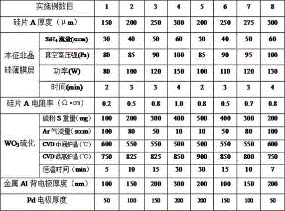
[0044] (1) Complete the basic etching and cleaning of the monocrystalline silicon wafer according to the above scheme. Among them, the thickness of the silicon wafer is 150 μm, and the resistivity is 0.2 Ω•cm.

[0045] (2) SiH is introduced into the PECVD system 4 , flow 30 sccm, pressure 80 Pa, time 2 min, power 80W.

[0046] (3) Place the quartz boat filled with sulfur powder S (100mg) in the low-temperature area upstream of the vent of the quartz tube of the heating furnace at a temperature of 250°C. WO 3 Place the silicon wafer in the center of the furnace, fill the quartz tube with protective gas Ar for 10 min to exhaust the air, and then heat the quartz tube to 600 °C. The Ar gas flow is 100 sccm.

[0047] (4) Keep the above-mentioned Ar gas flow constant, slowly heat the quartz tube to 750°C at 3°C / min, keep the temperature constant for 5 minutes, and then cool to room temperature.

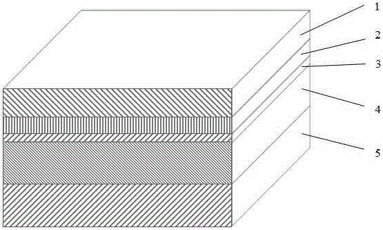
[0048] (5) Thermally evaporated Al electrodes on the back of the silicon wafer wi...

example 2

[0051] (1) Complete the etching and cleaning of the monocrystalline silicon wafer according to the above scheme. Among them, the thickness of the silicon wafer is 200 μm, and the resistivity is 0.5 Ω•cm.

[0052] (2) SiH is introduced into the PECVD system 4 , flow 40 sccm, pressure 85 Pa, time 3 min, power 100W.

[0053] (3) Place the quartz boat filled with sulfur powder S (200mg) in the low-temperature area upstream of the vent of the quartz tube of the heating furnace at a temperature of 230°C. WO 3 Place the silicon wafer in the center of the furnace, fill the quartz tube with protective gas Ar for 15 min to exhaust the air, and then heat the quartz tube to 550 °C. The Ar gas flow rate is 80 sccm.

[0054] (4) Keep the above-mentioned Ar gas flow constant, slowly heat the quartz tube to 825 °C at ~5 °C / min, keep the temperature for 10 min, and then cool to room temperature.

[0055] (5) Thermally evaporated Al electrodes on the back of the silicon wafer with tungste...


PUM

PropertyMeasurementUnit
thicknessaaaaaaaaaa
electrical resistivityaaaaaaaaaa
thicknessaaaaaaaaaa

Abstract

The invention discloses a preparation method for a tungsten disulfide / silicon (WS<2> / Si) heterojunction solar cell. The main process comprises the steps of cleaning and texturing a p type monocrystalline silicon wafer, and then putting the monocrystalline silicon wafer into a PECVD system to prepare an intrinsic amorphous silicon thin film layer; then carrying out WO<3> sulfuration to prepare a WS<2> thin film layer; and carrying out thermal evaporation of a metal aluminium back electrode on the back surface, and carrying out electron beam evaporation on the front surface to obtain an upper electrode formed by a palladium thin film to obtain the heterojunction solar cell. Due to a chemical vapor deposition method, the large-area, uniform-distribution and high-crystallinity nano WS<2> thin film material can be prepared, so that the advantages of high carrier mobility and adjustable band gap are realized; and in addition, the heterojunction solar cell is simple in experimental method, controllable in process, easy to operate, relatively low in cost, high in photoelectric conversion efficiency, and capable of realizing the effective conversion of solar energy.

Description

technical field [0001] The invention belongs to the technical field of microelectronics and optoelectronics, and more specifically relates to a preparation process of a tungsten disulfide / silicon heterojunction solar cell. Background technique [0002] In today's world, resource and environmental problems are becoming more and more prominent, and the global energy crisis and carbon emission problems are becoming more and more serious. Solar energy, as a clean energy source, has become a new energy source that is vigorously developed by various countries because of its renewability and no environmental pollution. The marked photovoltaic industry has developed rapidly, and the research and development of solar cells has become one of the fastest growing and most dynamic fields in recent years. Solar cell, also known as "solar chip" or "photovoltaic cell", is a photoelectric component that can convert energy. At present, two key issues restrict its development: improving conver...

Claims


Application Information

Patent Timeline
Patent Type & Authority Applications(China)
IPC IPC(8): H01L31/18H01L31/074
CPCH01L31/074H01L31/18Y02E10/50Y02P70/50
Inventor 曾祥斌王文照陈晓晓丁佳李寒剑徐素娥郭富城
Owner HUAZHONG UNIV OF SCI & TECH
Why Eureka
Try Eureka