
Method for preparing copper film through controlled atmosphere cold spraying
A technology of copper thin film and cold spraying, applied in the direction of pressure inorganic powder plating, etc., can solve the problems of serious sewage pollution of electrolytic copper foil, difficulty in satisfying the production of rigid copper clad laminates, and large production water consumption, so as to achieve uniform and controllable film thickness, Low cost of mass production, effect of preventing metal oxidation
- Summary
- Abstract
- Description
- Claims
- Application Information
AI Technical Summary
Problems solved by technology
Method used
Image

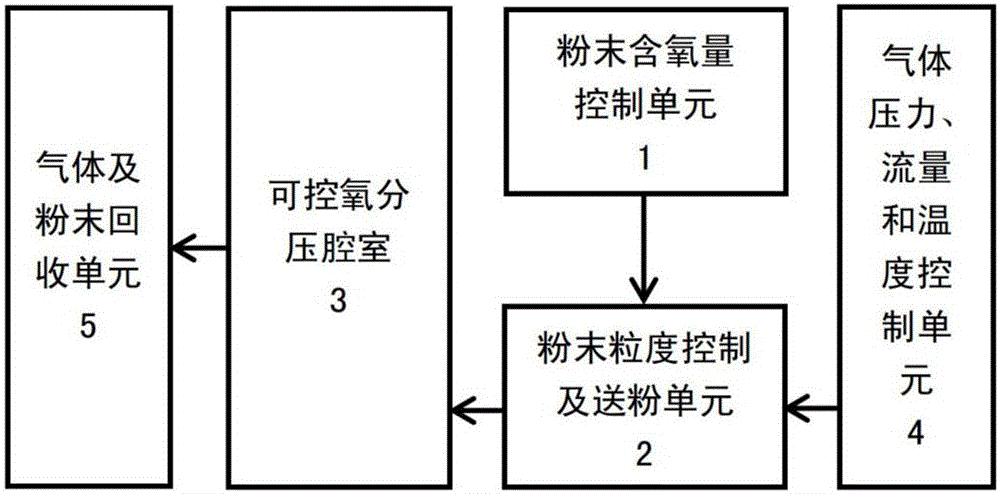
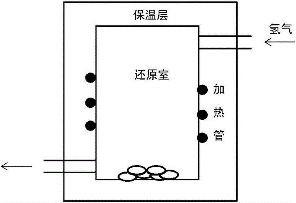
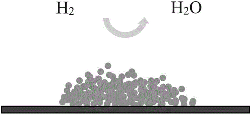
Examples
Embodiment 1
[0044] In this embodiment, spherical submicron pure copper powder is selected as the raw material, the particle size range of the original copper powder particles is 0.3-1.5 μm, a polished single crystal silicon wafer is selected as the substrate, helium is used as the carrier gas, and the gas pressure during spraying is 0.1MPa, the gas preheating temperature is 200°C, the spraying distance is 5mm, and the copper film is prepared on the single crystal silicon wafer by the controlled atmosphere cold spraying, the film thickness is about 10μm, Figure 4 It is a cross-sectional SEM photo of the copper thin film. From the cross-sectional morphology of the prepared copper thin film, it can be seen that the copper thin film is uniform, continuous, well bonded to the substrate, and has no cracks.
Embodiment 2
[0046] In this embodiment, spherical submicron pure copper powder is selected as the raw material, the particle size range of the original copper powder particles is 0.3-1.5 μm, a polished single crystal silicon wafer is selected as the substrate, helium is used as the carrier gas, and the gas pressure during spraying is 0.1MPa, the gas preheating temperature is 100°C, the spraying distance is 5mm, and the copper film is prepared on the single crystal silicon wafer by controlled atmosphere cold spraying, and the film thickness is about 7μm.
Embodiment 3
[0048]In this embodiment, spherical submicron pure copper powder is selected as the raw material, the particle size range of the original copper powder particles is 0.3-1.5 μm, a polished single crystal silicon wafer is selected as the substrate, helium is used as the carrier gas, and the gas pressure during spraying is 0.1MPa, the gas preheating temperature is 200°C, the spraying distance is 10mm, and the copper thin film pattern is prepared on the single crystal silicon wafer by controlled atmosphere cold spraying. The single line width of the pattern is 0.14±0.02mm, and the thickness is about 4μm. Figure 5 It is a photo of the copper thin film pattern. From the overall appearance of the prepared copper pattern, it can be seen that the copper pattern lines are uniform and continuous, and various required two-dimensional copper thin film patterns can be prepared according to requirements.
PUM
| Property | Measurement | Unit |
|---|---|---|
| Particle size | aaaaa | aaaaa |
Abstract
Description
Claims
Application Information