Transition metal chalcogenide homojunction, homojunction diode and preparation of homojunction

A technology of transition metal chalcogenides and compounds, applied in semiconductor/solid-state device manufacturing, electrical components, circuits, etc., can solve problems such as dopant shedding, affecting doping stability, and affecting the life of homojunctions, achieving high Softness and the effect of improving photoelectric conversion efficiency

Active Publication Date: 2017-03-29
UNIV OF SCI & TECH BEIJING
View PDF3 Cites 20 Cited by
  • Summary
  • Abstract
  • Description
  • Claims
  • Application Information

AI Technical Summary

Problems solved by technology

However, dopants physically adsorbed on the surface of the sample are susceptible to falling off due to environmental influences, thus affecting the doping stability.
Moreover, the dopant is easy to react with the surrounding active materials, so it also affects the life of the homojunction.

Method used


Image

  • Transition metal chalcogenide homojunction, homojunction diode and preparation of homojunction
  • Transition metal chalcogenide homojunction, homojunction diode and preparation of homojunction
  • Transition metal chalcogenide homojunction, homojunction diode and preparation of homojunction

Examples


Embodiment 1

[0032] A preparation method of transition metal chalcogenide homojunction, specifically comprising the following steps:

[0033] (1) Clean the silica substrate: put the 2.5*2.5cm silica substrate into acetone, ethanol, and deionized water successively, and after ultrasonic cleaning for 10 minutes in each solution, take it out and dry it with nitrogen;

[0034] (2) Chemical vapor deposition grows a single layer of molybdenum disulfide, using sulfur powder and molybdenum trioxide as reactants, preparing and depositing it on the surface of silicon dioxide cleaned in step (1) at 860°C to obtain molybdenum disulfide with a substrate Nanosheets; the formed monolayer molybdenum disulfide is a regular triangle, and the side length of the regular triangle is about 100 microns;

[0035] (3) Build a protective layer: Spin-coat PMMA glue (protective layer) on top of the molybdenum disulfide nanosheets with the substrate, and then expose half of the molybdenum disulfide nanosheets (unprote...

Embodiment 2

[0043] A preparation method of transition metal chalcogenide homojunction, specifically comprising the following steps:

[0044] (1) Clean the silicon dioxide substrate: put the molybdenum diselenide substrate into acetone, ethanol, and deionized water successively, and after ultrasonic cleaning in each solution for 10 minutes, take it out and dry it with nitrogen;

[0045] (2) Growth of monolayer molybdenum diselenide by chemical vapor deposition: after chemical vapor deposition onto the silicon dioxide surface cleaned in step (1), molybdenum diselenide nanosheets with a substrate are obtained;

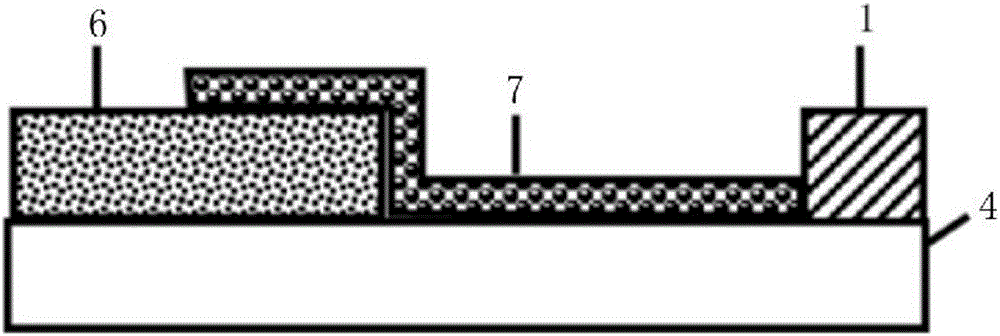
[0046] (3) Suspending a part of the molybdenum diselenide nanosheet area, soaking the unsuspended area of ​​the transition metal chalcogenide nanosheet in formic acid solution for 20-30min, and then cleaning it with deionized water to prepare Transition metal chalcogenide homojunctions.

Embodiment 3

[0048] A preparation method of a transition metal chalcogenide homojunction diode, specifically comprising the following steps:

[0049] (1) On a silicon dioxide substrate, pattern poly-3,4-ethylenedioxythiophene / polystyrenesulfonic acid (PEDOT:PSS) by suitable means; the patterning technique can be UV exposure or laser interference.

[0050] (2) Using traditional PMMA wet transfer method to transfer molybdenum disulfide nanosheets to the target substrate, during this process, dry and heat at 60°C to remove deionized water; assist in the realization of acid treatment repair;

[0051] (3) Using electron beam exposure technology, ultraviolet exposure ultraviolet or gold wire method, combined with electron beam evaporation and thermal evaporation deposition electrodes, to prepare transition metal chalcogenide homojunction diodes.

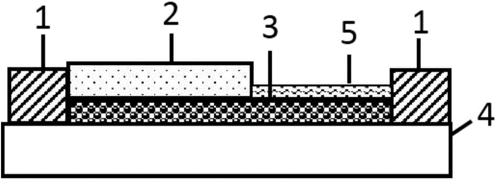
[0052] A transition metal chalcogenide homojunction diode, obtained by the above preparation method, the structure of the transition metal chalcogeni...


PUM


Abstract

The invention mainly belongs to the technical field of preparation of homojunction, and specifically relates to a transition metal chalcogenide homojunction and a preparation method thereof. According to the method, a transition metal chalcogenide nanosheet is used as a raw material, a protection layer is arranged on a part of area of the transition metal chalcogenide nanosheet for protection, and the unprotected area of the transition metal chalcogenide nanosheet is treated by an acid to repair the structural defects of the transition metal chalcogenide nanosheet so as to form the transition metal chalcogenide homojunction in the protected and unprotected areas of the transition metal chalcogenide nanosheet. The structure of the homojunction prepared from the method provided by the invention is scarcely influenced by the environment, has good stability and strong operability, requires no high temperature annealing and requires no doping process.

Description

technical field [0001] The invention mainly belongs to the technical field of homojunction preparation, and in particular relates to a transition metal chalcogen compound homojunction, a homojunction diode and a preparation method for the homojunction. Background technique [0002] Compared with the heterojunction, the homojunction brings smaller interfacial contact resistance, fewer carrier traps, good rectification characteristics and ultra-high photoelectric conversion efficiency due to its perfectly matched energy band structure. , optoelectronics and other fields have received extensive attention. On the other hand, two-dimensional nanomaterials represented by graphene have made important progress in the fields of electronics and optoelectronics since 2004. [0003] In 2011, B.Radisavljevic et al. from Switzerland discovered transition metal chalcogenides represented by monolayer molybdenum disulfide, which may become the next two-dimensional nanomaterial worth studyin...

Claims


Application Information

Patent Timeline
Patent Type & Authority Applications(China)
IPC IPC(8): H01L29/861H01L21/329H01L29/06H01L29/12
CPCH01L29/0688H01L29/12H01L29/6609H01L29/66128H01L29/861
Inventor 张跃张先坤张铮刘硕林沛申衍伟杜君莉柳柏杉
Owner UNIV OF SCI & TECH BEIJING
Why Eureka
Try Eureka