Manufacturing method of crystalline silicon solar cell resistant to PID effect

A technology of solar cells and manufacturing methods, which is applied in circuits, photovoltaic power generation, electrical components, etc., can solve problems such as accelerated aging of components and plastic pipelines, white spots on the appearance of batches, and ozone is harmful to the human body, and achieve low surface state Density, raw materials are non-toxic, and the effect of improving passivation effect

Inactive Publication Date: 2017-05-03
JIANGSU FOCUS NEW ENERGY TECH
View PDF4 Cites 2 Cited by
  • Summary
  • Abstract
  • Description
  • Claims
  • Application Information

AI Technical Summary

Problems solved by technology

This method has the advantage of rapid film formation, but there are still the following problems: a. Because the film formation speed is too fast, the resulting silicon dioxide film is relatively fragile, and it is prone to batch appearance of white spots, fingerprints and other undesirable problems, resulting in increased costs
b. Escaping ozone is harmful to the human body, and ozone waste gas that is not decomposed in time will also cause accelerated aging of some components and plastic pipelines in the equipment

Method used


Image

  • Manufacturing method of crystalline silicon solar cell resistant to PID effect

Examples


Embodiment 1

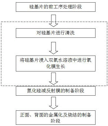
[0047] A kind of method using hydrogen peroxide to prepare anti-PID film, its step comprises:

[0048] (1) Etch and remove the edge of the diffused silicon wafer, wash and remove the phosphosilicate glass layer; the solution used for cleaning is hydrofluoric acid aqueous solution, the mass concentration of hydrofluoric acid aqueous solution is 8%, the solution temperature is 25 ° C, and the cleaning solution is The time is 50s;

[0049] (2) After 10 minutes, immerse the silicon wafer in a hydrogen peroxide solution to grow an oxide film. The temperature of the solution is 25°C, the concentration of hydrogen peroxide is 3%, the treatment time is 4 minutes, and the thickness of the ozone oxide layer is 2nm;

[0050] (3) After 10 minutes, deposit a silicon nitride film on the silicon wafer to be processed; the thickness of the silicon nitride film is 84 nm, and the refractive index is 2.08.

Embodiment 2

[0052] A kind of method using hydrogen peroxide to prepare anti-PID film, its step comprises:

[0053] (1) Etch and remove the edge of the diffused silicon wafer, wash and remove the phospho-silicate glass layer; use hydrofluoric acid aqueous solution for cleaning, the mass concentration of hydrofluoric acid aqueous solution is 5%, the solution temperature is 20°C, and the cleaning time is 150s;

[0054] (2) After 20 minutes, immerse the silicon wafer in a hydrogen peroxide solution to grow an oxide film. The temperature of the solution is 40°C, the concentration of hydrogen peroxide is 6%, the treatment time is 2 minutes, and the thickness of the formed silicon dioxide oxide layer is 4nm;

[0055] (3) After 30 minutes, deposit a silicon nitride film on the silicon wafer to be processed; the thickness of the silicon nitride is 81 nm, and the refractive index is 2.07.


PUM

PropertyMeasurementUnit
thicknessaaaaaaaaaa
thicknessaaaaaaaaaa
thicknessaaaaaaaaaa

Abstract

The invention discloses a manufacturing method of a crystalline silicon solar cell resistant to a PID effect. In the crystalline silicon solar cell resistant to the PID effect, a silicon dioxide layer is formed between a silicon substrate layer and a silicon nitride film. The manufacturing method comprises the following specific steps: carrying out front process treatment on the silicon substrate, wherein the treatment comprises the steps of affected layer removal and cleaning, texturing, diffusion and etching; carrying out phosphorosilicate glass removal and cleaning on the treated silicon substrate; soaking the cleaned silicon substrate into a hydrogen peroxide solution with certain concentration and temperature for oxidation treatment, taking out the silicon substrate after a certain period of time, drying after rinsing with deionized water to obtain the silicon dioxide layer; depositing a silicon nitride layer on the surface of a silicon oxide layer; and carrying out metallization and sintering on the front face and the back face of the silicon substrate. A silicon oxide film obtained by adopting a hydrogen peroxide oxidation technology is compact and has a relatively low surface state density, and the passivation effect for surface defects of base silicon is improved, so that the photoelectric conversion efficiency of the solar cell is improved.

Description

technical field [0001] The invention belongs to the field of manufacturing crystalline silicon solar cells, and in particular relates to a method for manufacturing an anti-PID effect crystalline silicon solar cell. Background technique [0002] Among all kinds of energy, solar energy has great development prospects due to its advantages of no pollution, large reserves, wide energy distribution and large market space. In recent years, the grid-connected system of photovoltaic power generation has been gradually popularized and applied. The scale of photovoltaic power generation system is getting larger and larger, and the system voltage is getting higher and higher. People have found a serious power attenuation phenomenon of photovoltaic modules, that is, the attenuation of power generation by components caused by the high voltage (600-1000V or even higher) between the photovoltaic module circuit and its grounded metal frame, which is called the potential-induced attenuation ...

Claims


Application Information

Patent Timeline
Patent Type & Authority Applications(China)
IPC IPC(8): H01L31/18
CPCH01L31/1804H01L31/1868Y02E10/547Y02P70/50
Inventor 马建峰刘强
Owner JIANGSU FOCUS NEW ENERGY TECH
Why Eureka
Try Eureka