Preparation method for silicon micro/nano structure based on mechanical carving and metal catalysis etching

A technology of mechanical scribing and metal catalysis, applied in microstructure technology, microstructure devices, manufacturing microstructure devices, etc., can solve the problems of high cost and difficulty in large-scale integrated manufacturing, and achieve the effect of small applied load

Inactive Publication Date: 2017-10-20
SOUTHWEST JIAOTONG UNIV
View PDF9 Cites 2 Cited by
  • Summary
  • Abstract
  • Description
  • Claims
  • Application Information

AI Technical Summary

Problems solved by technology

The structures processed by the "bottom-up" method are usually randomly distributed, which makes it difficult for large-scale integrated manufacturing
In the "top-down" processing method, the structure obtained by ultraviolet exposure (or electron beam exposure) is used as a mask, combined with the inductively coupled plasma etching process, silicon micro / nanostructures with high aspect ratio can be obtained, but the ultraviolet Exposure, e-beam exposure, and inductively coupled plasma etching all require specialized equipment and are expensive

Method used


Image

  • Preparation method for silicon micro/nano structure based on mechanical carving and metal catalysis etching

Examples


Embodiment 1

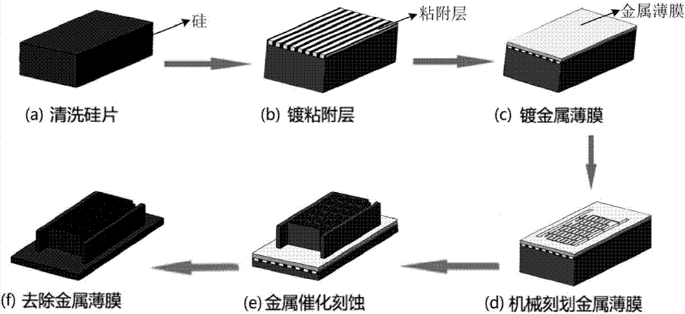
[0025] S1. Pretreatment of silicon wafer: Put the silicon wafer in acetone for ultrasonic cleaning for 5 minutes, then wash it with deionized water, then put the silicon wafer into ethanol solution for ultrasonic cleaning for 10 minutes, then rinse it with deionized water repeatedly and dry it with nitrogen. Get sample A;

[0026] S2. Integration of precious metal nano-film: A resistance thermal evaporation coating instrument (Wuhan Namei Technology Co., Ltd.) is used to integrate a titanium / silver nano-film on the surface of sample A. During the coating process, the thickness of the titanium nano-film is 2nm. When silver nano-film is plated, the vacuum degree of the coating instrument is set to 10 -4 Pa, the current is set to 110A, and a silver nano-film with a thickness of about 50nm is deposited to obtain sample B;

[0027] S3: Mechanical scribing of precious metal nano-films: Using multi-point contact micro-nano processing equipment, using a ball-point pen tip spherical steel b...

Embodiment 2

[0030] This embodiment is compared with the embodiment 1, except that in step S2, a different coating method is used to integrate the silver nano-film, the other steps are the same. In this embodiment, step S2 is specifically:

[0031] S2. Integrated silver nano-film: A magnetron sputtering machine (BEIYI JPGF 700A) is used to deposit a titanium / silver nano-film on the surface of sample A. The thickness of the adhesion layer titanium nano film is 2 nm. During the magnetron sputtering process, the radio frequency mode is adopted, the air pressure is set to 0.2Pa, and the power is set to 100W. After igniting, cover the sample with the baffle for about 3 minutes, and then remove the baffle after the oxide layer on the surface of the target material is removed. The coating time is set to 50s, the thickness of the obtained silver nano-film is about 50nm, and sample B is obtained.

Embodiment 3

[0033] This embodiment is compared with the embodiment 1, except that different types of nano-films are integrated in step S2, the other steps are the same. In this embodiment, step S2 is specifically:

[0034] S2. Integrated gold nano-film: using resistive thermal evaporation coater (Wuhan Namei Technology Co., Ltd.), deposit a titanium / gold nano-film on the surface of sample A, where the thickness of the adhesion layer is 2nm and the thickness of the gold nano-film Is 50 nm, and sample B is obtained.


PUM

PropertyMeasurementUnit
thicknessaaaaaaaaaa
thicknessaaaaaaaaaa
thicknessaaaaaaaaaa

Abstract

The invention discloses a preparation method for a silicon micro/nano structure based on mechanical carving and metal catalysis etching. The method comprises the following steps of S1, preprocessing a silicon wafer, cleaning the surface of the silicon wafer and then carrying out drying to obtain a sample A; S2, integrating noble metal nano-film, depositing an adhesion layer on the surface of the sample A and integrating the noble metal nano-film on the surface of the adhesion layer to obtain a sample B; S3, mechanically carving the noble metal nano-film, carving the surface of the sample B through mechanical carving and removing the carved part of the noble metal nano-film, thereby obtaining a sample C which is located at any required position and has a set shape pattern; and S4, preparing the silicon micro/nano structure, placing the sample C into mixed solution of hydrofluoric acid and hydrogen peroxide and etching the sample C, thereby obtaining the silicon micro/nano structure with a high aspect ratio. In general, the preparation method has the advantages that the cost is low, the operation is simple and the processing can be positioned. Mass production is hopeful.

Description

Technical field [0001] The invention belongs to the technical field of micro / nano structure manufacturing, and specifically relates to a silicon micro / nano structure preparation method based on mechanical scribing and metal catalytic etching. Background technique [0002] With the rapid development of micro-nano electromechanical systems, micro-sensing devices and micro-energy devices such as micro-lithium-ion batteries have received extensive attention. As the specific capacity of silicon is as high as 4200mAh / g, silicon micro / nano structures are now widely used in devices such as miniature lithium-ion batteries. Silicon micro / nano structures include silicon micro / nanowire structures, silicon micro / nano pillar structures, silicon micro / nanotube structures, and silicon nanospheres. Generally, the preparation methods of silicon micro / nano structures are divided into "top-down" etching methods and "bottom-up" deposition methods. The structures processed by the "bottom-up" method ...

Claims


Application Information

Patent Timeline
Patent Type & Authority Applications(China)
IPC IPC(8): B81C1/00B82Y30/00B82Y40/00
CPCB81C1/00619B82Y30/00B82Y40/00
Inventor 蒋淑兰王丰钱林茂武韩强余丙军
Owner SOUTHWEST JIAOTONG UNIV
Why Eureka
Try Eureka