Titanium nitride-based novel nano-structure photocathode

A nanostructure, titanium nitride technology, applied in nanotechnology for sensing, nano-optics, light-emitting cathode manufacturing, etc., can solve unfavorable electronic transition and tunneling emission, low external quantum efficiency of cathode, high material purchase cost, etc. problem, to achieve the effect of local electric field energy transmission, wide adjustable spectrum range, and improved probability and ability

Active Publication Date: 2017-10-20
SOUTHEAST UNIV
View PDF5 Cites 7 Cited by
  • Summary
  • Abstract
  • Description
  • Claims
  • Application Information

AI Technical Summary

Problems solved by technology

[0006] For conventional metal photocathodes, mainly including gold, silver, copper, aluminum and other materials, the existing problems in current theory and technology are: (1) The work function of ordinary conventional metals is relatively high (greater than 4.2eV), which is not conducive to electronic Transition and tunneling emission; (2) The reflectivity of visible and near-infrared light waves is very high for the planar metal cathode without structural design on the surface, and the external quantum efficiency of the cathode is very low; (3) The melting point of the metal is low ( Among them, copper is the highest at 1083°C), under the condition of high energy density and strong incident laser, the temperature rises with the generation of thermal effect, the cathode emitter is prone to damage and ablation, and the stability is poor; (4) gold and silver belong to Precious metal materials, corresponding to high material purchase costs

Method used


Image

  • Titanium nitride-based novel nano-structure photocathode
  • Titanium nitride-based novel nano-structure photocathode
  • Titanium nitride-based novel nano-structure photocathode

Examples


Embodiment 1

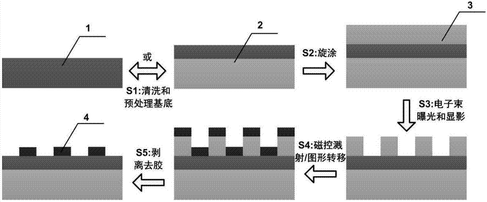
[0046] The present invention proposes a novel nanostructured photocathode and its preparation method, specifically, combining figure 1 As shown, the nanostructured photocathode of the present invention is prepared on a substrate material, such as a silicon wafer or a quartz substrate with a transparent conductive layer. Its concrete preparation method is as follows:

[0047] S1) process the base material:

[0048] For example, for quartz substrate materials, the surface is cleaned by ultrasonic cleaning with acetone, alcohol and deionized water in sequence, and then a transparent conductive oxide ITO thin film layer is prepared on the surface-cleaned quartz substrate material by magnetron sputtering. Specifically, for example, a 200 nm thick transparent conductive oxide ITO thin film layer is obtained by vapor deposition for 600 s under the condition of 100 W. The transparent conductive oxide of the present invention may also be fluorine-doped tin oxide (FTO) or aluminum-dop...

Embodiment 2

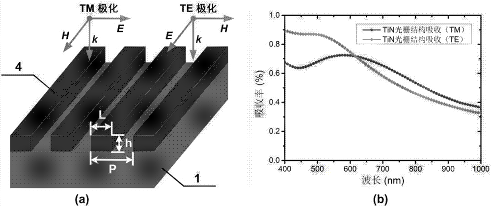
[0061] The invention discloses a photocathode based on a titanium nitride nano-grating structure, which combines figure 2 As shown, it adopts silicon chip as substrate 1, and the thickness of this substrate 1 is 500 μ m, adopts the method for embodiment 1 to prepare titanium nitride nano grating structure (sub-wavelength scale) on the surface then, and its width L is 150nm, and thickness h is 150nm, the period P is 300nm, and the duty cycle is 0.5. By solving the electromagnetic field, using the finite difference time domain (FDTD) method to simulate and simulate the absorption spectrum of the titanium nitride nanostructure layer in the present embodiment in the 400-1000nm band, as shown in the attached figure 2 As shown in (b), under the condition of TM (that is, the incident surface and the electric field direction perpendicular to the grating groove) polarized light irradiation, there is a resonant absorption peak at the light wave position of about 600nm, and the maximum...

Embodiment 3

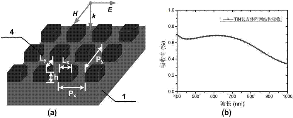
[0063] see image 3 , similar to Example 2, using the preparation process and method described in Example 1, the difference is that the titanium nitride nanostructure is a monodisperse nanostructure array, the width Lx and Ly are both 150nm, and the thickness h is 150nm. The period in the X-axis direction is 300nm, the duty ratio is 0.5, the period in the Y-axis direction is also 300nm, and the duty ratio is 0.5; the absorption of light waves by the titanium nitride nanostructure layer can be obtained by finite difference time domain simulation calculation situation, such as image 3 As shown in (b), there is a plasmon resonance absorption peak at about 650 nm, and the direction of the electric field E of the incident light wave vector is rotated by 90 degrees, and the obtained absorption spectrum is the same as image 3 It is exactly the same as shown in (b).


PUM

PropertyMeasurementUnit
thicknessaaaaaaaaaa
widthaaaaaaaaaa
electrical resistivityaaaaaaaaaa

Abstract

The invention discloses a titanium nitride-based novel nano-structure photocathode, and the titanium nitride photocathode includes a substrate and a titanium nitride nano-structure layer. The invention also relates to a method for preparing the titanium nitride photocathode and an electric field assisting type photocathode test device, and the electric field assisting type photocathode includes an insulating spacer, a metal sheet anode, an upper/lower electrode lead and an external bias power supply. The core titanium nitride nano-structure in the design has a surface Plasmon resonance effect, brings photon absorption enhancement and local electric field enhancement, a material work function is only about 3.7eV and electrical conductivity is excellent, thereby contributing to emission of photoinduced electrons; and through design of constituting nano patterns and structure parameters of the titanium nitride structure, plasmon resonance matched with incident excitation light waves can be obtained, thereby realizing electron emission capable of being controlled by light. Since the titanium nitride material also has stable physico-chemical properties, the photocathode provided by the invention is stable and efficient.

Description

[0001] Field [0002] The invention relates to a novel nanostructure photocathode based on titanium nitride material, an electric field assisted photocathode and a preparation method thereof, mainly utilizing the surface plasmon resonance enhancement effect of the titanium nitride material and its unique physical properties, The invention is applied to an electron source and belongs to the technical field of photoelectric devices. Background technique [0003] The photocathode electron source is the core component of the next-generation free electron laser, linear accelerator and Compton scattering source, and its basic characteristics are low emittance, low energy dissipation and ultra-high current density. The existing mainstream practical photocathodes mostly use alkali metals (alloys) with low work functions or III-V compound semiconductor materials with negative electron affinity, and their quantum efficiency is relatively high (10 -2 ~10 -1 ), but the above materials a...

Claims


Application Information

Patent Timeline
Patent Type & Authority Applications(China)
IPC IPC(8): H01J1/34H01J9/12B82Y15/00B82Y20/00B82Y30/00
CPCB82Y15/00B82Y20/00B82Y30/00H01J1/34H01J9/12H01J2201/3421
Inventor 王琦龙齐志央徐林田润知张建屠彦
Owner SOUTHEAST UNIV
Why Eureka
Try Eureka