Hole transport layer containing organic conjugated polymer semiconductor material and application thereof
A technology of hole transport layer and conjugated polymer, which is applied in the field of electronic devices with photoelectric conversion characteristics, can solve the problems of time consumption, achieve the effects of improving performance, simplifying structure and synthesis, and reducing costs
- Summary
- Abstract
- Description
- Claims
- Application Information
AI Technical Summary
Problems solved by technology
Method used
Image

Examples
Embodiment 1
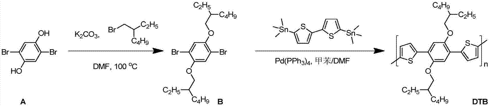
[0052] Synthesis of conjugated polymer DTB based on p-alkoxybenzene and dithiophene:
[0053] Synthetic route such as figure 1 Shown. First, the H atom in the -OH group of p-phenylene glycol is replaced with an alkyl group, and then the product is copolymerized with the distannide of dithiophene to obtain the target polymer DTB.
[0054] Product B: Raw material A (2.0 g) and anhydrous potassium carbonate (4.13 g) were added to a pre-dried 250 ml flask, followed by vacuum and argon filling operations, and repeated twice. Then DMF (37 ml) was added, and bromoisooctane (3.6 g) was added all at once after the mixed system was dissolved. After that, the flask was stirred at 100°C for 20 hours. After the reaction system is cooled to room temperature, it is concentrated using a rotary evaporator, and then the organic layer is extracted, washed with water, and concentrated. Finally, the product is further purified by silica gel column chromatography to obtain the final product. 2.3 gra...
Embodiment 2
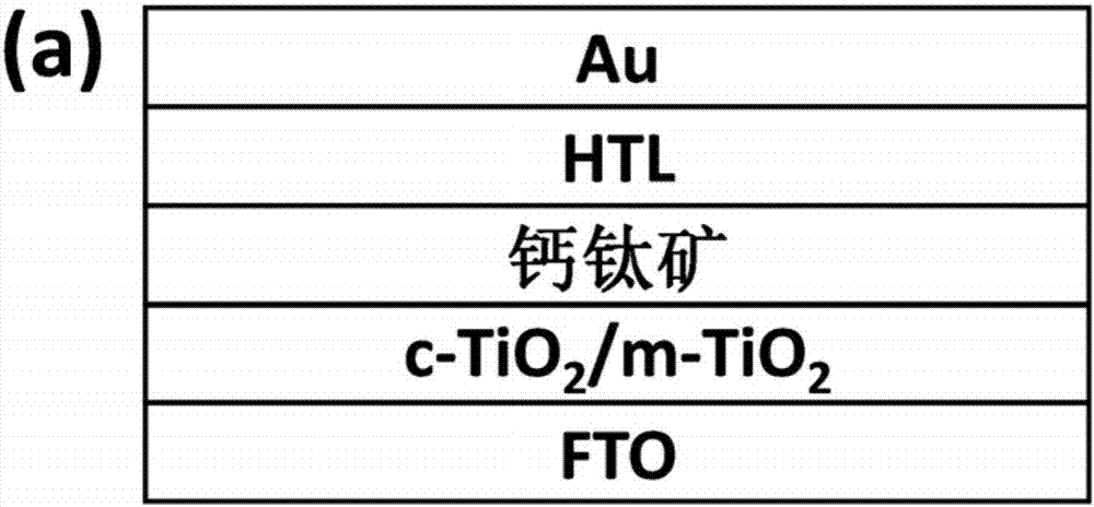
[0057] Preparation of photoelectric devices containing polymer DTB
[0058] Preparation with FTO / c-TiO 2 / m-TiO 2 / Perovskite / HTL / Au structure photoelectric devices, such as Figure 2a As shown (which is specifically a schematic diagram of the formal structure of a perovskite solar cell), where FTO (fluorine-doped tin oxide) is the bottom layer; c-TiO 2 / m-TiO 2 Dense TiO without pinholes 2 Layer and mesoporous TiO 2 Layer; HTL is a hole transport layer, which is the hole transport layer of DTB.
[0059] The manufacturing process of optoelectronic devices is summarized as follows:
[0060] First, clean the FTO glass (Nippon Sheet Glass) with detergent, deionized water, acetone and ethanol, and ultrasonically treat it in an ultrasonic bath for 30 minutes. After that, the FTO glass was treated in an ultraviolet ozone device for 30 minutes. Prepare 0.15M diisopropoxylate bis(acetylacetone) diacetate in n-butanol solution, then use spin coating method to coat the cleaned FTO glass at 20...
Embodiment 3
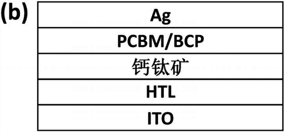
[0062] Preparation of photoelectric devices containing polymer DTB
[0063] Preparation of optoelectronic devices with ITO / HTL / perovskite / PCBM / BCP / Ag structure, such as Figure 2b As shown (which is specifically a schematic diagram of the trans structure of a perovskite solar cell). Among them, ITO (indium-doped tin oxide) is the bottom layer; HTL is the hole transport layer, which is the hole transport layer of DTB; PCBM is a fullerene derivative; BCP is 2,9-dimethyl-4, 7-Biphenyl-1,10-phenanthroline.
[0064] The manufacturing process of optoelectronic devices is summarized as follows:
[0065] First, clean the ITO glass (Nippon Sheet Glass) with detergent, deionized water, acetone and ethanol, and ultrasonically treat it in an ultrasonic bath for 30 minutes. After that, the ITO glass was treated in an ultraviolet ozone device for 30 minutes. DTB was dissolved in chlorobenzene (30 mg / ml) and preheated at 80°C to prepare a hole transport layer (HTL) by spin-coating the DTB soluti...
PUM
| Property | Measurement | Unit |
|---|---|---|
| current density | aaaaa | aaaaa |
Abstract
Description
Claims
Application Information
 - R&D
- Intellectual Property
- Life Sciences
- Materials
- Tech Scout
- Unparalleled Data Quality
- Higher Quality Content
- 60% Fewer Hallucinations
Browse by: Latest US Patents, China's latest patents, Technical Efficacy Thesaurus, Application Domain, Technology Topic, Popular Technical Reports.
© 2025 PatSnap. All rights reserved.Legal|Privacy policy|Modern Slavery Act Transparency Statement|Sitemap|About US| Contact US: help@patsnap.com