Preparation method of silicon substrate array with nanometer gaps being controllable and application thereof

A nano-gap and array technology, applied in the field of nano-gap array materials, can solve the problems of complex preparation method, small construction area, poor repeatability, etc., and achieve the effects of simple process, large construction area and clean surface

Active Publication Date: 2018-06-12
HEFEI INSTITUTES OF PHYSICAL SCIENCE - CHINESE ACAD OF SCI
View PDF7 Cites 12 Cited by
  • Summary
  • Abstract
  • Description
  • Claims
  • Application Information

AI Technical Summary

Problems solved by technology

Utilizing the surface-enhanced Raman effect is expected to realize the rapid trace detection of the concentration of sodium saccharin, but the substrate materials that produce the surface-enhanced Raman effect in the prior art are mainly noble metal nanoparticles such as gold and silver. These noble metal nanoparticles not only The structure area is small, the repeatability is poor, the uniformity is poor, and the preparation method is complicated and the cost is high, so the application of the surface-enhanced Raman effect is largely limited

Method used


Image

  • Preparation method of silicon substrate array with nanometer gaps being controllable and application thereof
  • Preparation method of silicon substrate array with nanometer gaps being controllable and application thereof
  • Preparation method of silicon substrate array with nanometer gaps being controllable and application thereof

Examples


preparation example Construction

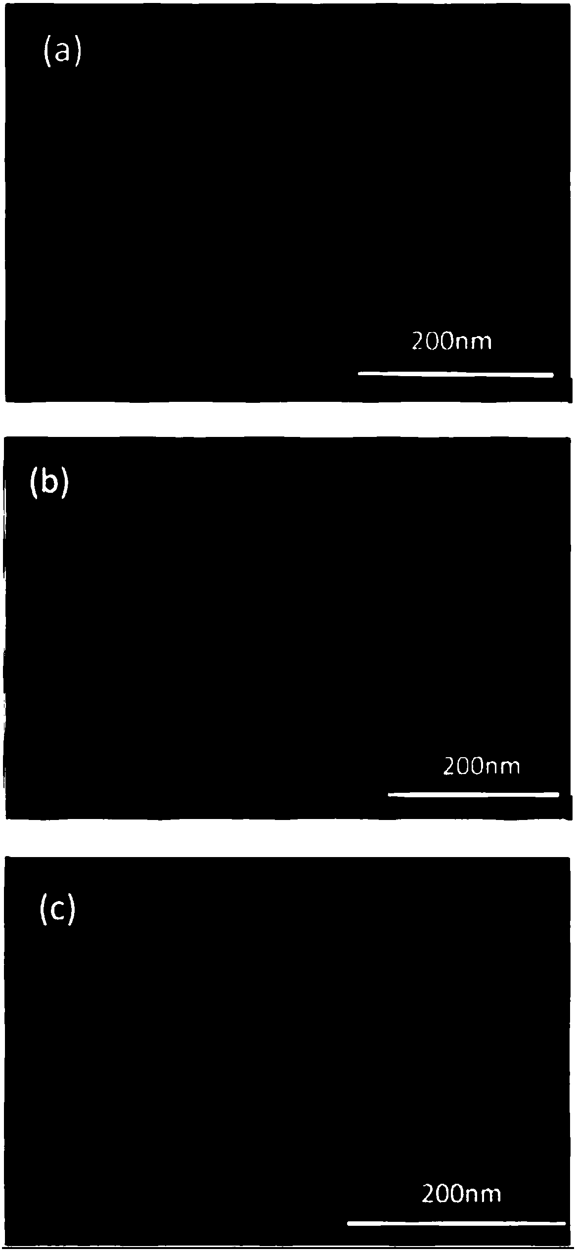
[0029] Such as Figure 4 As shown, a method for preparing a silicon-based array with controllable nano-gap includes the following steps:

[0030] Step A: Prepare a closely arranged single-layer polystyrene colloidal crystal array on the silicon wafer substrate to obtain a single-layer polystyrene colloidal crystal array on the silicon wafer substrate.

[0031] Step B: Use reactive ion etching to etch the single-layer polystyrene colloidal crystal array on the silicon wafer substrate, and remove the single-layer polystyrene colloidal crystal array on the silicon wafer substrate after the etching is completed, to obtain Conical silicon-based array.

[0032] Step C. Using the tapered silicon-based array as a template, a layer of gold film with a thickness of 10-50nm is deposited on the surface of the template by physical deposition method, and gold nanospheres are deposited on the top of the tapered silicon-based, through The deposition time is controlled to adjust the gap of the gold...

Embodiment approach

[0034] (1) The preparation of a closely arranged single-layer polystyrene colloidal crystal array on a silicon wafer substrate includes the following steps:

[0035] Step A1. Put the silicon wafer substrate into acetone, ethanol, the first mixed solution, and deionized water in sequence for ultrasonic cleaning, and then dry the cleaned silicon wafer substrate, and then place it in an ultraviolet ozone cleaning machine for 10 ~40min to obtain a silicon wafer substrate with a hydrophilic surface. Wherein, the first mixed solution is formed by mixing concentrated sulfuric acid with a mass concentration of 1.84 g / ml and hydrogen peroxide with a mass concentration of 1.1 g / ml in a volume ratio of 3:1.

[0036] Step A2. Put the silicon wafer substrate with hydrophilic surface into the ethanol diluent of polystyrene colloidal spheres, and use the gas-liquid interface self-assembly method to prepare tightly arranged monolayer polystyrene on the silicon wafer substrate Colloidal crystal ar...

Embodiment 1

[0047] Such as Figure 4 As shown, a method for preparing a silicon-based array with controllable nano-gap may specifically include the following steps:

[0048] Step a1. Put the silicon wafer substrate into acetone, ethanol, and the first mixed solution (the first mixed solution consists of concentrated sulfuric acid with a mass concentration of 1.84 g / ml and hydrogen peroxide with a mass concentration of 1.1 g / ml in a volume ratio of 3. :1), ultrasonic cleaning in deionized water, and then drying the cleaned silicon wafer substrate, and then placing it in an ultraviolet ozone cleaning machine and irradiating it for 10-40 minutes to obtain a silicon wafer with a hydrophilic surface Base.

[0049] Step b1. Take a polystyrene colloidal sphere suspension (2.5wt%) with a polystyrene colloidal sphere diameter of 120nm, mix it with ethanol in equal volume, and then perform ultrasonic oscillation treatment for 10-30 minutes to obtain a uniformly dispersed polystyrene Styrene colloidal ...


PUM

PropertyMeasurementUnit
thicknessaaaaaaaaaa
thicknessaaaaaaaaaa

Abstract

The invention discloses a preparation method of a silicon substrate array with nanometer gaps being controllable and application thereof. The preparation method comprises the steps that a silicon slice substrate single-layer polystyrene colloidal crystal array is prepared; etching is conducted on the silicon slice substrate single-layer polystyrene colloidal crystal array by adopting a reactive ion etching method, the single-layer polystyrene colloidal crystal array is removed after etching is completed, and a tapered silicon substrate array is prepared; and the tapered silicon substrate arrayis taken as a template, a layer of gold film with the thickness being 10-50nm is deposited on the surface of the template by adopting a physical deposition method, gold nanoballs are deposited and formed at the top of the tapered silicon substrate, the distances among the gold nanoballs are adjusted by controlling the deposition time, and the silicon substrate array with the nanometer gaps beingcontrollable is prepared by controlling the deposition time and adjusting the distances among the gold nanoballs. The silicon substrate array is large in structure area, clean on surface, high in sensitivity and good in detection performance, can directly serve as a substrate material which has long-term stability and a high-activity surface enhanced Raman effect, and can be used for conducting rapid trace detection on the concentration of saccharin sodium salt. The preparation method is simple, convenient to operate, low in cost and economical and environmentally friendly.

Description

Technical field [0001] The invention relates to the field of nanogap array materials, in particular to a preparation method and application of a silicon controlled nanogap array. Background technique [0002] Sodium saccharin is a commonly used synthetic sweetener with the longest history and most controversy in the food industry. It is widely used in beverages, jellies, preserves, pastries and other food industries. Saccharin sodium does not have any nutritional value to the human body except that it can cause sweetness in taste. When eating too much sodium saccharin, it will affect the normal secretion of gastrointestinal digestive enzymes, reduce the absorption capacity of the small intestine, cause loss of appetite, and cause thrombocytopenia, cause symptoms such as acute hemorrhage, multiple organ damage, and even cause malignant poisoning events. In addition, saccharin sodium has certain carcinogenicity. Long-term consumption can cause malnutrition of young people and nega...

Claims


Application Information

Patent Timeline
Patent Type & Authority Applications(China)
IPC IPC(8): G01N21/65B82Y30/00B82Y40/00C23C14/16C23C14/30C23C14/35
CPCB82Y30/00B82Y40/00C23C14/16C23C14/165C23C14/30C23C14/35G01N21/658
Inventor 杨绍松刘广强赵倩郭静蔡伟平
Owner HEFEI INSTITUTES OF PHYSICAL SCIENCE - CHINESE ACAD OF SCI
Why Eureka
Try Eureka