Condensed-ring n-type polymer with main chain containing cyano indanone and application of condensed-ring n-type polymer
A technology of cyanoindanone and polymer, which is applied in the field of polymer optoelectronic materials, can solve the problems of insufficient absorption spectrum and low absorption coefficient, and achieve the goals of improving photocurrent and battery device efficiency, increasing absorption coefficient, and optimizing short-circuit current Effect
- Summary
- Abstract
- Description
- Claims
- Application Information
AI Technical Summary
Problems solved by technology
Method used
Image
Examples
Embodiment 1
[0039] Embodiment 1: the preparation of polymer P1~P5
[0040] Add monomer M1 (0.5 mmol) and monomer M4 (0.5 mmol) into a 25 mL two-necked flask, pass through nitrogen protection, and add 8 mL of toluene. Add 5mg Pd(PPh 3 ) 4 , After reacting at 95°C for 12h, the polymer was precipitated with methanol and washed three times. Obtain dark colored polymer P1, yield 85.7%, 1HNMR(CDCl3 500MHz):δ:7.00-7.48(m,18H),4.13-3.50(m,8H),1.05-1.30(br,112H),0.87(t,12H).GPC:Mn=27.8kDa,Mw = 70.3 kDa, PDI = 2.53. Elem. Anal.: C, 77.05; H, 8.45; N, 2.90; O, 1.66; S, 9.95. The reaction formula is as follows:
[0041]
[0042] Add monomer M2 (0.5mmol) and monomer M4 (0.5mmol) into a 25mL two-necked flask, pass through nitrogen protection, and add 12mL of toluene. After pumping twice, add 7mg of Pd(PPh3)4, react at 95°C for 12h, precipitate the polymer with methanol, and wash three times. Obtain dark colored polymer P2, yield 84.9%, 1 HNMR(CDCl3 500MHz):δ:7.02-7.48(m,16H),4.12-3.60(m,14H)...
Embodiment 2
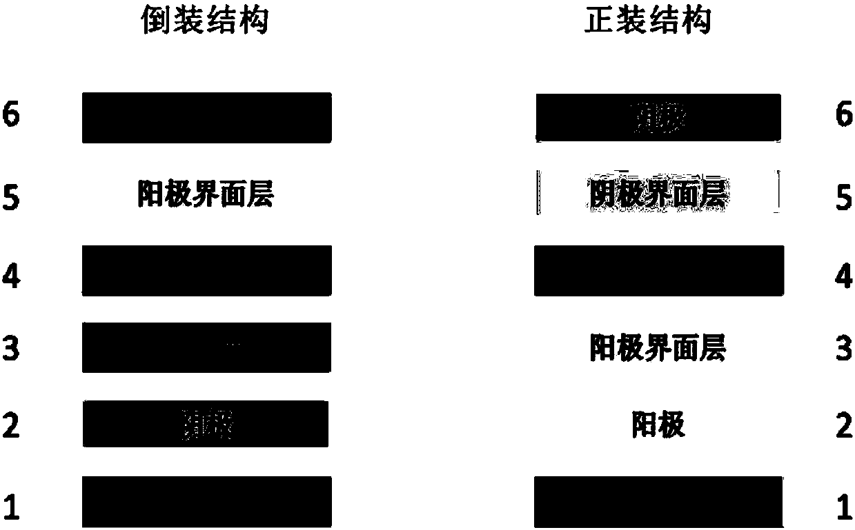
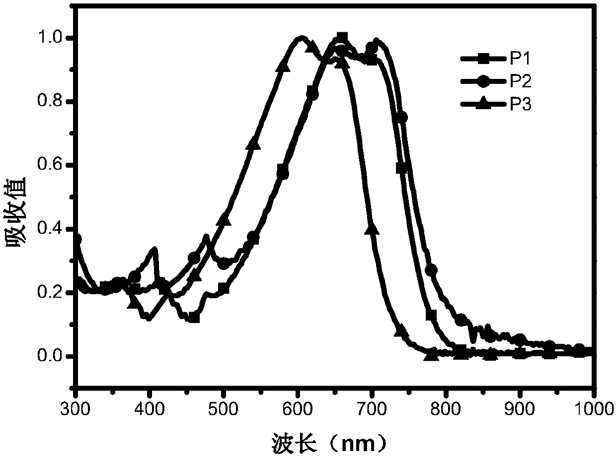
[0051] Embodiment 2: Polymer P1, P2, P3 (the AB component is the same in the structure) is used in the organic photovoltaic device (ITO negative electrode / cathode interface layer / active layer / positive machine interface layer / anode) as electron acceptor
[0052] Pre-cut the ITO conductive glass with a square resistance of 20 ohms / cm2 into 15mm×15mm square pieces. Use acetone, special detergent for micron-sized semiconductors, deionized water, and isopropanol to clean ultrasonically in sequence, blow nitrogen whistle, and place in a constant temperature oven for later use. Spin-coat a layer of PFN-Br with a thickness of 5nm on the ITO, and then spin-coat the active layer materials PTB7-Th / P1, PTB7-Th / P2, PTB7-Th / P3 (the mass ratio of the donor PTB7-Th to the acceptor Both are 1:2), the thickness is 110 nm, and MoO is finally evaporated 3 and Al electrodes. All preparations were carried out in a glove box under a nitrogen atmosphere. The current-voltage curves of the fabricate...
Embodiment 3
[0053] Embodiment 3: Polymer P1, P2, P3 (the AB component is the same in the structure) is used in organic photovoltaic device (ITO anode / anode interface layer / active layer / cathode interface layer / cathode) as electron acceptor
[0054] Pre-cut the ITO conductive glass with a square resistance of 20 ohms / cm2 into 15mm×15mm square pieces. Use acetone, special detergent for micron-sized semiconductors, deionized water, and isopropanol to clean ultrasonically in sequence, blow nitrogen whistle, and place in a constant temperature oven for later use. Spin-coat a layer of 20nm thick PEDOT:PSS (poly-3,4-ethylenedioxythiophene / polystyrene sulfonate) on ITO, and then spin-coat active layer materials PTB7-Th / P1, PTB7-Th / P2 , PTB7-Th / P3 (in which the mass ratio of donor PTB7-Th and acceptor is 1:2), and the thickness is 100 nm. Then spin-coat a layer of PFN-Br with a thickness of 5nm, and finally evaporate Al electrodes. All preparations were carried out in a glove box under a nitrogen...
PUM
| Property | Measurement | Unit |
|---|---|---|
| Thickness | aaaaa | aaaaa |
Abstract
Description
Claims
Application Information


