Monocrystalline silicon surface composite microstructure based on full-wave band anti-reflection and a preparation method thereof

A technology of surface compounding and monocrystalline silicon, applied in the field of photovoltaics, can solve the problems such as the inability to realize the utilization of long-wavelength solar energy, and achieve the effects of improving utilization, improving conversion efficiency, and optimizing structure

Active Publication Date: 2019-06-07
NANJING UNIV OF AERONAUTICS & ASTRONAUTICS
View PDF14 Cites 6 Cited by
  • Summary
  • Abstract
  • Description
  • Claims
  • Application Information

AI Technical Summary

Problems solved by technology

Its invention has improved the optical performance of crystalline silicon solar cells to a certain extent, but the working band is still only in the short-wave region, and it is impossible to realize the utilization of long-wave solar energy

Method used


Image

  • Monocrystalline silicon surface composite microstructure based on full-wave band anti-reflection and a preparation method thereof
  • Monocrystalline silicon surface composite microstructure based on full-wave band anti-reflection and a preparation method thereof
  • Monocrystalline silicon surface composite microstructure based on full-wave band anti-reflection and a preparation method thereof

Examples


preparation example Construction

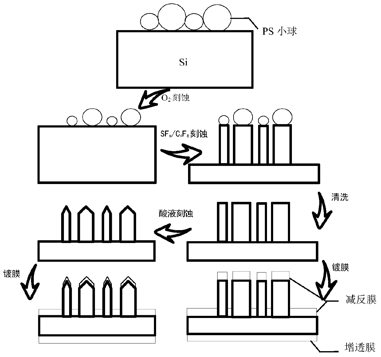
[0038] Such as figure 1 Shown is a flow chart of the present invention. A method for preparing a single crystal silicon surface composite microstructure based on full-band anti-reflection of the present invention includes part or all of the following steps (1) to (4), wherein each step is performed one or more times;

[0039](1) Silicon-based mask: Hydrophilic treatment of silicon wafers, preparation of a mixed solution of polystyrene beads, masking of silicon wafers after hydrophilic treatment, laying with a propulsion syringe, dripping sodium lauryl sulfate Solution, and use the pulling method to complete the mask, then air-dry the mask plate naturally, and then vacuum-dry it for 3 to 5 hours, and lay polystyrene beads on the surface of the silicon wafer;

[0040] Preferably, the steps of hydrophilic treatment of silicon wafers are: take single crystal silicon, wash, and cut the sample; place in a mixed solution of concentrated sulfuric acid and hydrogen peroxide, and heat ...

Embodiment 1

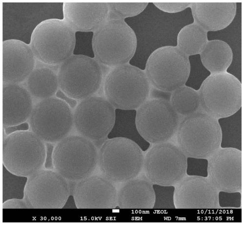
[0052] Example 1: Fabrication of nanopillar array structures with mixed diameters.

[0053] Select a 100mm×100mm circular double-sided polished P-type single crystal silicon, slice it with a diamond silicon wafer knife, and make a 25mm×25mm square silicon wafer substrate; mix the silicon wafer with concentrated sulfuric acid and hydrogen peroxide with a mass ratio of 7:3 Heat bath at 90°C for one hour in the solution to complete the hydrophilic treatment; prepare a mixed solution of polystyrene (Polystyrene, abbreviated as PS) beads: PS beads solution with a particle size of 400nm, PS beads solution with a particle size of 600nm, deionized Water and absolute ethanol are mixed according to the volume ratio of 0.5:0.5:3:7, and the mixture is ultrasonically oscillated at room temperature for 5 minutes; preparation of sodium dodecyl sulfate (SDS) solution: take 1 gram of sodium dodecyl sulfate 20mL deionized water, ultrasonic vibration for 20 minutes to dissolve it; take a 9mm×9mm...

Embodiment 2

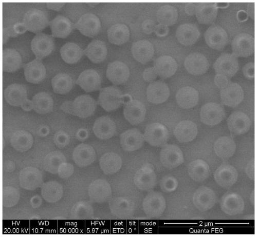
[0054] Example 2: Fabrication of Mixed Diameter Nano-Pencil Array Structure.

[0055] Select a 100mm×100mm circular double-sided polished P-type single crystal silicon, slice it with a diamond silicon wafer knife, and make a 25mm×25mm square silicon wafer substrate; mix the silicon wafer with concentrated sulfuric acid and hydrogen peroxide with a mass ratio of 7:3 Heat bath in the solution at a temperature of 90°C for one hour to complete the hydrophilic treatment; prepare a mixed solution of polystyrene (Polystyrene, abbreviated as PS) beads: a solution of nmPS beads with a particle size of 400, a solution of nmPS beads with a particle size of 600, and Ionized water and absolute ethanol are mixed according to the volume ratio of 0.5:0.5:3:7, and the solution is ultrasonically oscillated at room temperature for 5 minutes; preparation of sodium dodecyl sulfate (SDS) solution: take 1 gram of sodium dodecyl sulfate and put it in 20mL deionized water, ultrasonic vibration for 20 ...


PUM

PropertyMeasurementUnit
Film thicknessaaaaaaaaaa
Particle sizeaaaaaaaaaa

Abstract

The invention discloses a monocrystalline silicon surface composite microstructure based on full-band anti-reflection and a preparation method of the monocrystalline silicon surface composite microstructure. The preparation method comprises a part of or all of the following steps (1) - (4), and each step is executed for one or more times: (1) carrying out hydrophilic treatment on a silicon wafer,preparing a polystyrene sphere mixed solution, and paving a mask, polystyrene spheres, on the surface of the silicon wafer; (2) introducing oxygen for etching the wafer, and then introducing sulfur hexafluoride and octafluorocycloalkane for an etching-passivation-etching circulation to obtain monocrystalline silicon with a nano-pillar structure; (3) soaking the monocrystalline silicon with the nano-pillar structure into an acidic etching solution containing silver nitrate for surface corrosion to obtain monocrystalline silicon with a nano pencil-shaped structure; (4) carrying out magnetron sputtering on the monocrystalline silicon with the microstructure for plating an anti-reflection layer on the front surface, or the back surface or both, of the monocrystalline silicon. According to theinvention, the anti-reflection effect on full-band solar energy is effectively improved, so that the conversion efficiency of the solar cell is improved.

Description

technical field [0001] The invention belongs to the field of photovoltaic technology, and in particular relates to a composite microstructure on the surface of a monocrystalline silicon solar cell based on full-band solar antireflection and a preparation method thereof. Background technique [0002] As an important research direction of new energy technology, the utilization of solar radiation energy has attracted increasing attention from researchers at home and abroad. Solar cells are the most direct way to utilize solar energy, among which silicon cells are still used as the longest developing and most widely used solar cells. [0003] With the continuous improvement of various preparation technologies, research activities on silicon-based solar cells are very active at home and abroad. In terms of the preparation of the surface microstructure of solar cells, the current research work at home and abroad mainly focuses on simple microstructures. However, current studies ...

Claims


Application Information

Patent Timeline
IPC IPC(8): C30B33/12C30B33/10C30B29/06C23C14/35C23C14/10C23C14/08H01L31/0236H01L31/18B82Y40/00
CPCY02E10/50Y02P70/50
Inventor 杨理理李铖
Owner NANJING UNIV OF AERONAUTICS & ASTRONAUTICS
Why Eureka
Try Eureka