Eureka AIR delivers breakthrough ideas for toughest innovation challenges, trusted by R&D personnel around the world.

X-band gallium nitride based predistortion integrated circuit and manufacturing method

A technology of integrated circuit and manufacturing method, which is applied in the field of radio frequency, can solve the problems of power amplifier power supply efficiency, power output capability, and cost rise, etc., and achieve the effects of improving adjacent channel interference, high output power density, and easy manufacturing equipment

Active Publication Date: 2020-02-04
XIDIAN UNIV
View PDF5 Cites 0 Cited by
  • Summary
  • Abstract
  • Description
  • Claims
  • Application Information

AI Technical Summary

Problems solved by technology

However, the power supply efficiency and power output capability of the power amplifier cannot be fully utilized, resulting in an increase in cost; in addition, for this method, after falling back to a predetermined level, the improvement range reaches a peak value, but this peak value is limited. linearity of the amplifier itself

Method used


Image

  • X-band gallium nitride based predistortion integrated circuit and manufacturing method
  • X-band gallium nitride based predistortion integrated circuit and manufacturing method
  • X-band gallium nitride based predistortion integrated circuit and manufacturing method

Examples


Embodiment 1

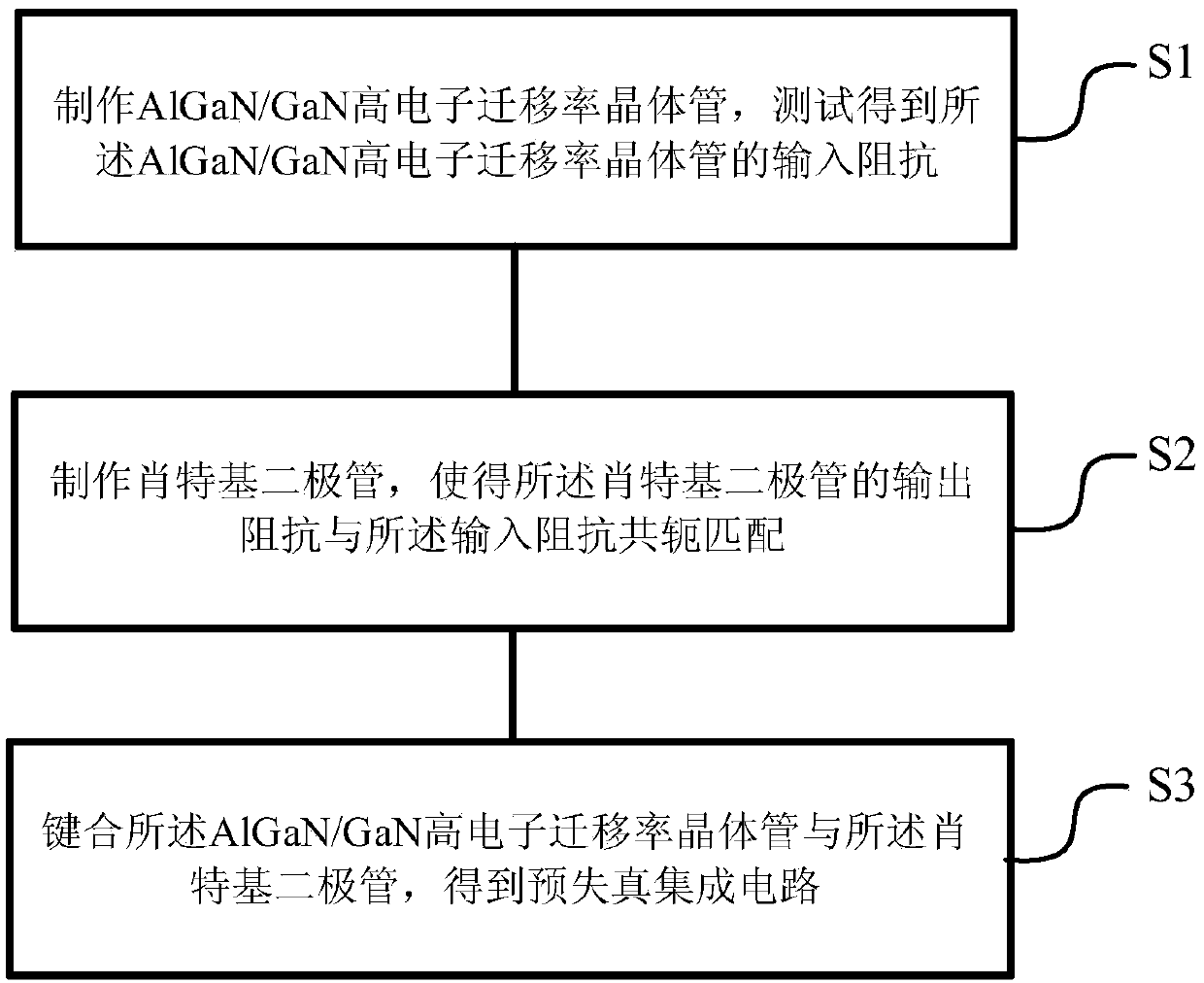
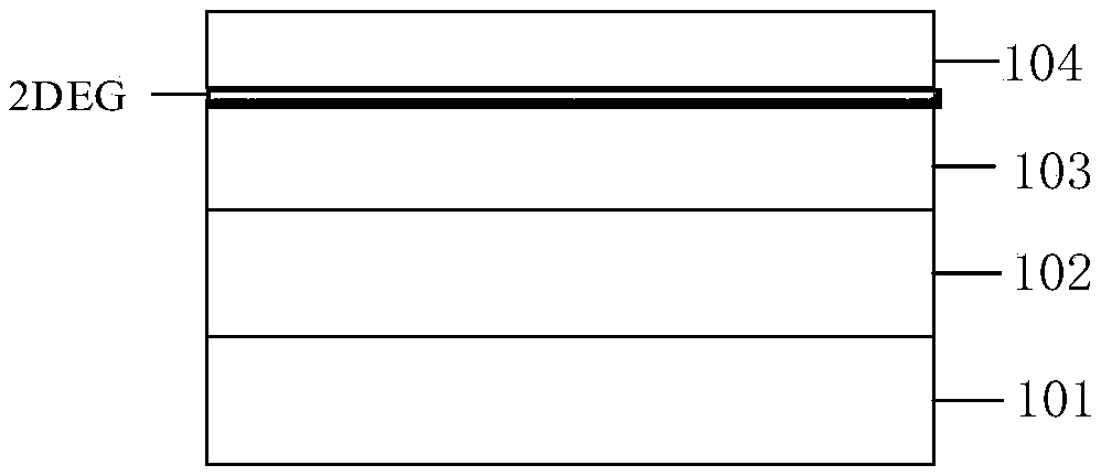
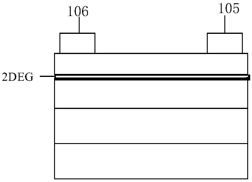
[0052] See figure 1 , figure 1 It is a flowchart of a manufacturing method of an X-band GaN-based predistortion integrated circuit according to an embodiment of the present invention. AlGaN / GaN high electron mobility transistors are fabricated on a sample wafer including a first substrate layer 101, a nucleation layer 102, a GaN buffer layer 103 and an AlGaN barrier layer 104, see Figure 2a , wherein a two-dimensional electron gas (Two dimensional electrons, 2DEG) exists between the buffer layer 103 and the barrier layer 104 . In the embodiment of the present invention, the first substrate layer 101 includes SiC, and the nucleation layer 102 includes AlN. First, clean the sample. The cleaning steps are as follows: place the sample in acetone for 2 minutes, and then boil it in a positive glue stripping solution heated in a water bath at 60°C for 10 minutes. After cleaning the remaining acetone and ethanol with deionized water, the sample was cleaned with HF solution for 30 ...

Embodiment 2

[0115] See Figure 3a-Figure 3h , Figure 3a-Figure 3h It is a schematic diagram of the manufacturing method of the Schottky diode according to the embodiment of the present invention.

[0116] According to the measured input impedance of the AlGaN / GaN HEMT device, the output impedance of the Schottky diode is Z d = r 1 +jxΩ, the junction capacitance of the Schottky diode can be calculated from the output impedance, and the junction capacitance of the Schottky diode is:

[0117]

[0118] It is known from the junction capacitance that the junction area and GaN doping concentration of the Schottky diode affect its size, thereby controlling the output impedance of the Schottky diode. Therefore, the Schottky diode is manufactured by controlling the junction area and GaN doping concentration of the Schottky diode. Teky diode.

[0119] Schottky diodes are fabricated on a second substrate layer 201 with a defined size. The second substrate layer 201 in the embodiment of the pr...

Embodiment 3

[0164] The specific steps of the manufacturing method of the predistortion integrated circuit of the embodiment of the present invention are as follows:

[0165] S301. Pretreat the AlGaN / GaN high electron mobility transistor.

[0166] Treat the surface of AlGaN / GaN HEMT devices, through AP3000 treatment liquid and baking, to enhance adhesion;

[0167] S302. Spin-coat a bonding material on the surface of the AlGaN / GaN high electron mobility transistor to form a bonding layer.

[0168] The bonding material of an embodiment of the present invention includes benzocyclobutene (BCB).

[0169] S303, exposing and developing the bonding layer to form a bonding pattern.

[0170] S3031. Set the exposure and development conditions according to the corresponding film thickness, expose the HEMT device spin-coated with BCB material, the photolithographic layout has bonding alignment marks, form a bonding pattern after development, and place the wafer on the hot plate bake.

[0171] S3032...


PUM

PropertyMeasurementUnit
thicknessaaaaaaaaaa
thicknessaaaaaaaaaa
depthaaaaaaaaaa

Abstract

The invention relates to a manufacturing method of an X-band gallium nitride based predistortion integrated circuit. The manufacturing method comprises the following steps of manufacturing an AlGaN / GaN high electron mobility transistor, and testing to obtain the input impedance of the AlGaN / GaN high electron mobility transistor; manufacturing a Schottky diode so that the output impedance and the input impedance of the Schottky diode can be in conjugated matching; and bonding the AlGaN / GaN high electron mobility transistor and the Schottky diode to obtain the predistortion integrated circuit. The predistortion integrated circuit provided by the embodiment of the invention not only can be effectively developed in low-frequency and narrow-band signals, but also can effectively output power inhigh-frequency and wide-band environments; meanwhile, the predistortion integrated circuit can improve the nonlinear distortion of a power amplifier and meet the index requirements of a communicationsignal electromagnetic environment simulator on harmonic waves and intermodulation components.

Description

technical field [0001] The invention belongs to the field of radio frequency technology, and in particular relates to an X-band gallium nitride-based predistortion integrated circuit and a manufacturing method. Background technique [0002] With the rapid development of modern wireless communication, limited spectrum resources need to carry higher and higher data traffic, and the 5G communication era requires higher transmission rates, and the design and work of wireless transmission systems will be under tremendous pressure. The core component of the wireless transmission system—the microwave power amplifier is generally in a nonlinear working state, and the modulated signal with changing envelope will produce intermodulation distortion after passing through the nonlinear microwave power amplifier, causing serious intersymbol interference and adjacent channel interference. At present, most of the second and third harmonics of modulation signals at home and abroad use switch...

Claims


Application Information

Patent Timeline
Patent Type & Authority Applications(China)
IPC IPC(8): H01L21/50H01L25/18
CPCH01L25/18H01L25/50
Inventor 马晓华杨凌芦浩周小伟祝杰杰侯斌宓珉翰郝跃
Owner XIDIAN UNIV
Why Eureka
Eureka Blog
Learn More