
Composite material and preparation method thereof and quantum dot light-emitting diode

A composite material and molar weight technology, applied in the field of nanomaterials, can solve the problems of unsatisfactory effect of electron transport materials, and achieve the effects of reducing donor ionization energy, increasing electrical conductivity, and self-compensating suppression.

Active Publication Date: 2020-02-04
TCL CORPORATION
View PDF6 Cites 1 Cited by
  • Summary
  • Abstract
  • Description
  • Claims
  • Application Information

AI Technical Summary

Problems solved by technology

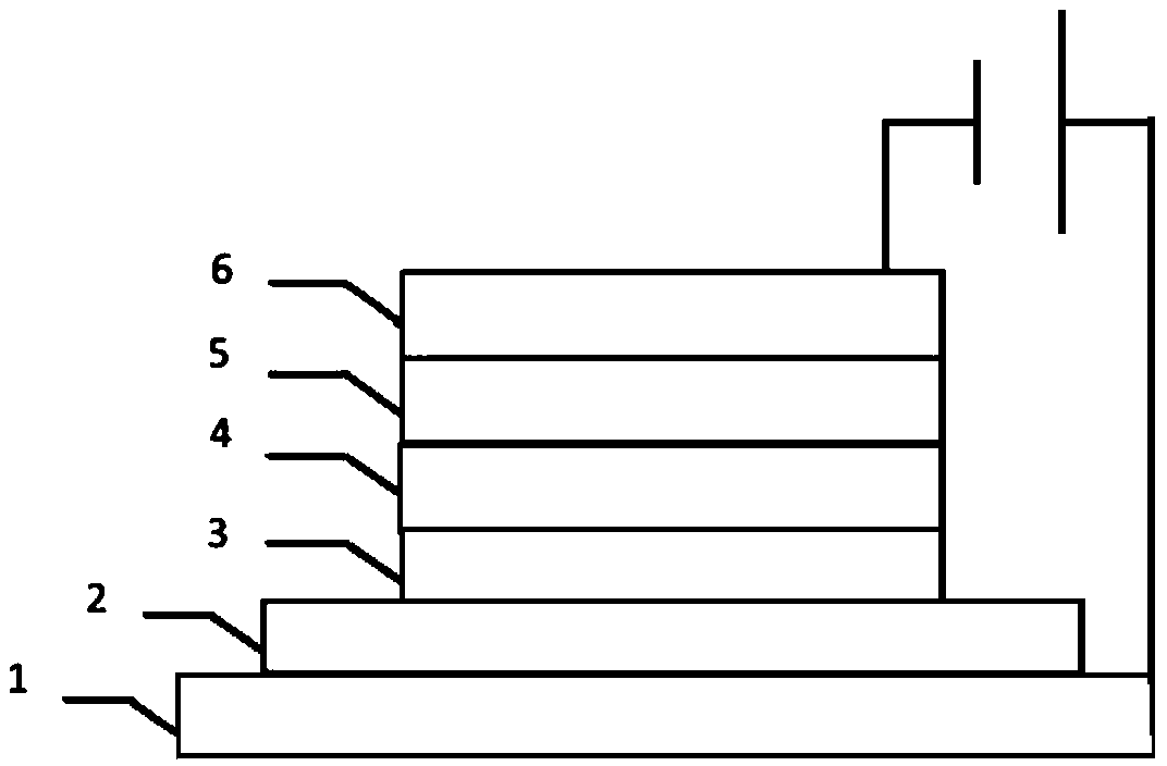
[0005] The purpose of the present invention is to overcome the above-mentioned shortcomings of the prior art, provide a composite material and its preparation method and quantum dot light-emitting diodes, aiming at solving the technical problem that the existing n-type ZnS has an unsatisfactory effect as an electron transport material

Method used


Image

  • Composite material and preparation method thereof and quantum dot light-emitting diode

Examples


preparation example Construction

[0021] On the other hand, the embodiment of the present invention also provides a method for preparing a composite material, comprising the following steps:

[0022] S01: Provide zinc salt, gallium salt, precursor salt containing selenium element and precursor salt containing sulfur element;

[0023] S02: dissolving the zinc salt, gallium salt, selenium-containing element precursor salt and sulfur-containing element precursor salt in a solvent, and performing heat treatment to obtain a precursor solution;

[0024] S03: Annealing the precursor solution to obtain the composite material.

[0025] In the composite preparation method provided in the embodiment of the present invention, the precursor solution is first prepared by using zinc salt, gallium salt, precursor salt containing selenium element and precursor salt containing sulfur element, and then the precursor solution is annealed to obtain a A kind of composite material of acceptor (Se)-donor (Ga) co-doped ZnS nanopartic...

Embodiment 1

[0049] Taking zinc chloride, sodium selenide, gallium chloride, ethanol, and sodium sulfide as examples, the preparation method of Se-Ga / ZnS composite material will be introduced in detail below.

[0050] 1) Add appropriate amount of zinc chloride, sodium selenide and gallium chloride to 50ml of ethanol to form a solution with a total concentration of 0.5M, wherein the molar ratio of zinc: selenium + gallium is 1:0.005; the molar ratio of selenium: gallium The ratio is 1:3. Stir at 70°C to dissolve.

[0051] 2) add the solution that sodium sulfide is dissolved in 10ml ethanol (molar ratio, S 2- :M x+ =1:1, M is zinc and gallium). Stirring was continued at 70 °C for 4 h to obtain a homogeneous solution.

[0052] 3) After the solution is cooled, spin-coat the treated ITO with a homogenizer and anneal at 250°C.

Embodiment 2

[0054] Taking zinc nitrate, potassium selenide, gallium nitrate, propanol, and potassium sulfide as examples, the preparation method of Se-Ga / ZnS composite material will be introduced in detail below.

[0055] 1) Add appropriate amount of zinc nitrate, potassium selenide and gallium nitrate to 50ml of propanol to form a solution with a total concentration of 0.5M, wherein the molar ratio of zinc: selenium + gallium is 1:0.005; the molar ratio of selenium: gallium It is 1:3. Stir to dissolve at 80°C.

[0056] 2) Add the solution that potassium sulfide is dissolved in 10ml propanol (molar ratio, S 2- :M x+ =1.1:1, M is zinc and gallium). Stirring was continued at 80 °C for 3 h to obtain a homogeneous solution.

[0057] 3) After the solution is cooled, spin-coat the treated ITO with a coater and anneal at 250°C.


PUM


Abstract

The invention belongs to the technical field of nano materials, and particularly relates to a composite material, a preparation method thereof and a quantum dot light-emitting diode. The composite material comprises ZnS nano-particles and Se and Ga elements doped in the ZnS nano-particles. The composite material is the Zns nanoparticles co-doped by the acceptor (Se)-donor (Ga), the doping of the Se-Ga in the composite material can improve the free carrier concentration of ZnS, so that the resistance of ZnS is reduced, the conductivity is increased, and the electron transmission capability of the composite material is finally improved; and the composite material can be used as a QLED electron transmission material, so that the effective compounding of electrons-holes in a quantum dot lightemitting layer can be promoted, the influence on the device performance by the exciton accumulation can be reduced, and the performance of the device and display performance are improved.

Description

technical field [0001] The invention belongs to the technical field of nanometer materials, and in particular relates to a composite material, a preparation method thereof and a quantum dot light-emitting diode. Background technique [0002] Semiconductor quantum dots have a quantum size effect. People can adjust the size of quantum dots to achieve the required specific wavelength of light. The emission wavelength of CdSe QDs can be tuned from blue light to red light. In traditional inorganic electroluminescent devices, electrons and holes are injected from the cathode and anode respectively, and then recombine in the light-emitting layer to form excitons to emit light. Conduction band electrons in wide bandgap semiconductors can be accelerated under high electric field to obtain high enough energy to hit QDs to make them emit light. [0003] In recent years, the use of inorganic semiconductors as electron transport layers has become a relatively hot research topic. Nano-Z...

Claims


Application Information

Patent Timeline
Patent Type & Authority Applications(China)
IPC IPC(8): H01L51/50H01L51/54B82Y30/00
CPCB82Y30/00H10K50/115H10K50/165
Inventor 何斯纳吴龙佳吴劲衡
Owner TCL CORPORATION
Learn More