

Manufacturing method of semiconductor photoelectronic device
A technology for optoelectronic devices and manufacturing methods, applied in semiconductor devices, electrical components, circuits, etc., can solve the problems of increasing the non-radiative recombination rate of devices, reducing the usable area of Micro-LED devices, color distortion, etc., and eliminating optical crosstalk of devices. problems, improve the luminous efficiency of the device, and improve the effect of the effective use area
- Summary
- Abstract
- Description
- Claims
- Application Information
AI Technical Summary
Problems solved by technology
Method used
Image

Examples
Embodiment 1
[0051] Example 1: Micro-LED formal installation structure
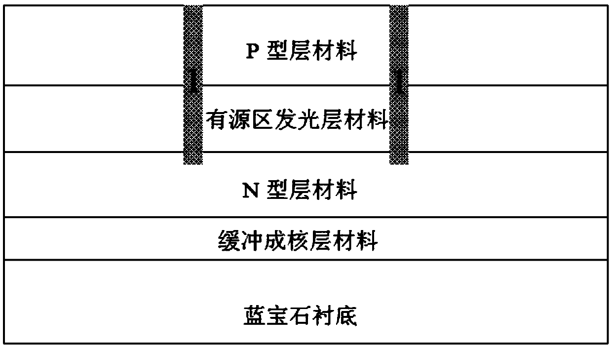
[0052] see reference Figure 1-5 , a Micro-LED chip front-loading structure based on ion implantation. The specific preparation process steps are as follows:
[0053] Step 1: Using MOCVD (metal organic chemical vapor deposition) on the sapphire substrate material to epitaxially grow the buffer nucleation layer material, N-type layer material, active region light-emitting layer material and P-type layer material to form an LED structure;
[0054] Step 2: Use a photoresist (or silicon dioxide, silicon nitride, metal aluminum, etc.) mask to define an ion implantation region, and form a high-resistance implantation isolation region 1 by hydrogen (or helium, nitrogen, fluorine) ion implantation, Adjust the energy and dose of implanted ions to precisely control the ion implantation depth, so that the implanted isolation region 1 penetrates the P-type layer and the light-emitting layer in the active region, so as to enter t...
Embodiment 2
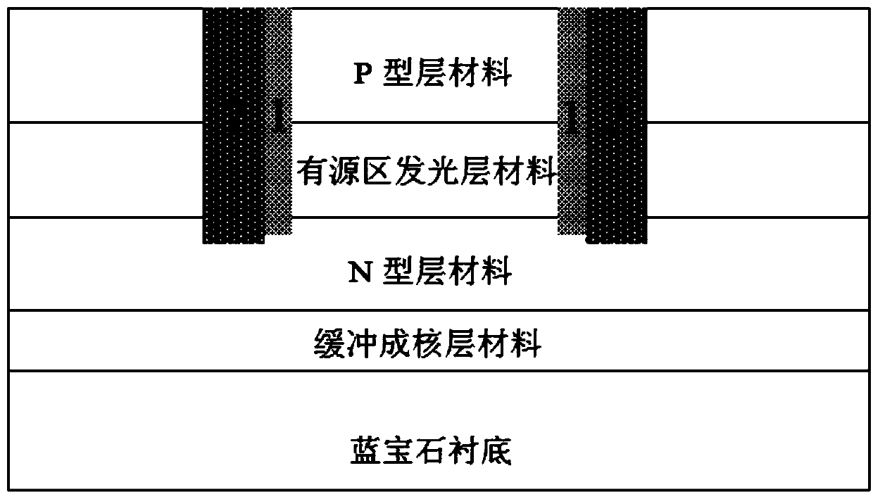
[0060] Example 2: Micro-LED formal installation structure
[0061] Please refer to Figure 6-7 , a Micro-LED chip front-loading structure based on ion implantation. The specific preparation process steps are as follows:
[0062] Step 1: On the sapphire substrate, use MOCVD (metal organic chemical vapor deposition) to epitaxially grow buffer nucleation layer material, high resistance layer material, N-type layer material, active region light-emitting layer and P-type layer material to form LED structure;
[0063] Step 2: use a photoresist (or silicon dioxide, silicon nitride, metal aluminum, etc.) mask to define an ion implantation region, and form a high-resistance implantation isolation region 4 by hydrogen (or helium, nitrogen, fluorine) ion implantation, Adjust the energy and dose of implanted ions to precisely control the ion implantation depth, so that the implanted isolation region 4 penetrates the P-type layer and the material of the light-emitting layer in the active...
Embodiment 3
[0069] Example 3: Micro-LED vertical structure
[0070] Please refer to Figure 8-9 , the specific preparation process steps of the vertical structure of the Micro-LED chip based on ion implantation are as follows:
[0071] Step 1: Using MOCVD (metal organic chemical vapor deposition) to epitaxially grow N-type layer material, active region light-emitting layer and P-type layer material in sequence on GaN or SiC substrate to form an LED structure;
[0072] Step 2: Use a photoresist mask to define the ion implantation area, form a high-resistance ion implantation isolation area 7 through hydrogen (or helium, nitrogen, fluorine) ion implantation, adjust the energy and dose of implanted ions to precisely control the ion implantation depth , so that the depth of the implanted isolation region 7 completely penetrates the GaN or SiC substrate, forming an isolation for the LED device;
[0073] Step 3: Further performing secondary ion implantation on the ion implantation isolation r...
PUM
 Abstract
Description
Claims
Application Information