A kind of interface atomic memristor and preparation method thereof
A memristor and interface technology, applied in the field of microelectronics, can solve problems such as poor consistency, high power consumption, and complicated operation, and achieve the effects of reducing defects and vacancies, low power consumption, and improving consistency
- Summary
- Abstract
- Description
- Claims
- Application Information
AI Technical Summary
Problems solved by technology
Method used
Image
Examples
preparation example Construction
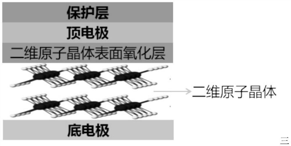
[0063] The method for preparing another interface-type atomic memristor based on two-dimensional atomic crystals includes the following steps:
[0064] 1) Prepare graphene or other semi-metallic two-dimensional atomic crystal materials by mechanical exfoliation method or chemical vapor deposition method;
[0065] 2) using ultraviolet lithography or electron beam lithography to prepare and design the shape of the bottom electrode of graphene or other semi-metallic two-dimensional atomic crystal materials on the substrate;
[0066] 3) Using an etching process, the excess graphene or other semi-metallic two-dimensional atomic crystal materials are etched cleanly;
[0067] 4) Preparation of two-dimensional atomic crystal materials by means of mechanical lift-off, chemical vapor deposition (CVD), chemical vapor transport (CVT), molecular beam epitaxy (MBE) or laser thinning;
[0068] 5) using oxygen ion treatment, natural oxidation, thermal oxidation or ultraviolet ozone treatment...
Embodiment 1
[0088] 1) Preparation of gold bottom electrode: first spin a layer of AZ5214 photoresist on the substrate with a glue spinner at 1500 r / min for 15 seconds and 4000 r / min for 30 s, and expose a strip of AZ5214 photoresist with a photolithography machine. Electrode pattern (line width is about 3μm), the pattern is revealed with developer, then 30nm gold electrode is grown on the substrate by electron beam evaporation, and finally put into acetone, alcohol and deionized water respectively to remove excess photoresist .
[0089] 2) Preparation and transfer of hafnium diselenide dielectric: using mechanical peeling method to peel off the hafnium diselenide thin film to SiO 2 On the surface of the / Si substrate, the thickness of the thin film is about 20 nm, and then the surface treatment of hafnium diselenide is performed by the oxygen ion treatment method, and the thickness of the oxide layer is about 5 nm.
[0090] 3) Transfer the hafnium diselenide thin film on the substrate to...
Embodiment 2
[0099] 1) Preparation of gold bottom electrode: first spin a layer of AZ5214 photoresist on the substrate with a glue spinner at 1500 r / min for 15 seconds and 4000 r / min for 30 s, and expose a strip of AZ5214 photoresist with a photolithography machine. Electrode pattern (line width is about 3μm), the pattern is revealed with developer, and then 30nm gold electrode is grown on the substrate by electron beam evaporation, and finally put into acetone, alcohol and deionized water, respectively, to remove excess photoresist .
[0100] 2) Preparation and transfer of titanium diselenide dielectric: the titanium diselenide film was exfoliated to SiO by mechanical exfoliation 2 On the surface of the / Si substrate, the thickness of the film is about 20 nm, and then the titanium diselenide is surface-treated by a surface oxidation treatment method.
[0101] 3) Transfer the titanium diselenide film on the substrate to the gold bottom electrode prepared in step 1).
[0102]4) Preparatio...
PUM
| Property | Measurement | Unit |
|---|---|---|
| thickness | aaaaa | aaaaa |
| thickness | aaaaa | aaaaa |
| thickness | aaaaa | aaaaa |
Abstract
Description
Claims
Application Information
 - R&D
- Intellectual Property
- Life Sciences
- Materials
- Tech Scout
- Unparalleled Data Quality
- Higher Quality Content
- 60% Fewer Hallucinations
Browse by: Latest US Patents, China's latest patents, Technical Efficacy Thesaurus, Application Domain, Technology Topic, Popular Technical Reports.
© 2025 PatSnap. All rights reserved.Legal|Privacy policy|Modern Slavery Act Transparency Statement|Sitemap|About US| Contact US: help@patsnap.com


