Interface type atomic memristor and preparation method thereof

A memristor and interface technology, applied in the field of microelectronics, can solve problems such as complex operation, high power consumption, and poor consistency, and achieve the effects of improving consistency, low power consumption, and reducing defects and vacancies

Active Publication Date: 2020-04-17
HUAZHONG UNIV OF SCI & TECH
View PDF11 Cites 6 Cited by
  • Summary
  • Abstract
  • Description
  • Claims
  • Application Information

AI Technical Summary

Problems solved by technology

[0005] In view of the defects of the prior art, the purpose of the present invention is to solve the technical problems of high power consumption, complex operation and poor consistency of existing memristor devices

Method used


Image

  • Interface type atomic memristor and preparation method thereof
  • Interface type atomic memristor and preparation method thereof
  • Interface type atomic memristor and preparation method thereof

Examples


preparation example Construction

[0063] The preparation method of another interface-type atomic memristor based on a two-dimensional atomic crystal comprises the following steps:

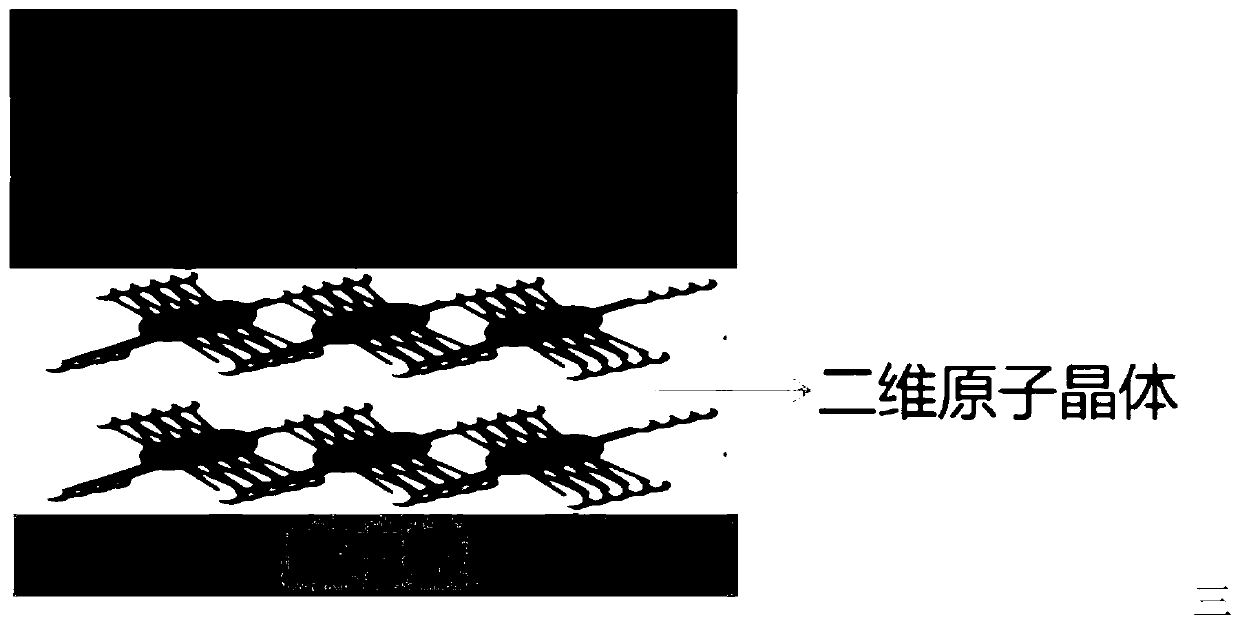
[0064] 1) Prepare graphene or other semi-metallic two-dimensional atomic crystal materials by mechanical exfoliation or chemical vapor deposition;

[0065] 2) Using ultraviolet lithography or electron beam lithography to prepare and design the shape of the bottom electrode of graphene or other semi-metallic two-dimensional atomic crystal materials on the substrate;

[0066] 3) Using an etching process to etch away excess graphene or other semi-metallic two-dimensional atomic crystal materials;

[0067] 4) Two-dimensional atomic crystal materials are prepared by mechanical exfoliation, chemical vapor deposition (CVD), chemical vapor transport (CVT), molecular beam epitaxy (MBE) or laser thinning;

[0068] 5) Surface oxidation treatment of two-dimensional atomic crystals is carried out by means of oxygen ion treatment, natural oxida...

Embodiment 1

[0088] 1) Preparation of gold-bottom electrodes: Firstly, spin-coat a layer of AZ5214 photoresist on the substrate with a coater at 1500 rpm for 15 seconds and at 4000 rpm for 30 seconds, and expose the strip-shaped electrodes with a photolithography machine. Electrode pattern (the line width is about 3 μm), the pattern is developed with a developer, and then a 30nm gold electrode is grown on the substrate by means of electron beam evaporation, and finally put into acetone, alcohol and deionized water respectively to remove excess photoresist .

[0089] 2) Preparation and transfer of hafnium diselenide dielectric: the hafnium diselenide film was peeled off to SiO by mechanical stripping 2 / Si substrate surface, the thickness of the film is about 20nm, and then the hafnium diselenide is surface treated by the oxygen ion treatment method, and the thickness of the oxide layer is about 5nm.

[0090] 3) Transfer the hafnium diselenide thin film on the substrate to the gold bottom ...

Embodiment 2

[0099] 1) Preparation of gold-bottom electrodes: Firstly, spin-coat a layer of AZ5214 photoresist on the substrate with a coater at 1500 rpm for 15 seconds and at 4000 rpm for 30 seconds, and expose the strip-shaped electrodes with a photolithography machine. Electrode pattern (the line width is about 3 μm), the pattern is developed with a developer, and then a 30nm gold electrode is grown on the substrate by means of electron beam evaporation, and finally put into acetone, alcohol and deionized water respectively to remove excess photoresist .

[0100] 2) Preparation and transfer of titanium diselenide dielectric: peel off the titanium diselenide film to SiO2 by mechanical stripping 2 / Si substrate surface, the thickness of the film is about 20nm, and then the titanium diselenide is surface treated by surface oxidation treatment.

[0101] 3) Transfer the titanium diselenide thin film on the substrate to the gold bottom electrode prepared in step 1).

[0102]4) Preparation o...


PUM

PropertyMeasurementUnit
Thicknessaaaaaaaaaa
Thicknessaaaaaaaaaa
Thicknessaaaaaaaaaa

Abstract

The invention discloses an interface type atomic memristor and a preparation method thereof. The memristor structurally comprises a sandwich structure with a bottom electrode / dielectric layer / top electrode on a substrate and a protective layer at the topmost part, the bottom electrode is made of inert metal materials such as platinum, gold and palladium, and flexible conductive materials such as indium tin oxide, graphene and other semimetal type two-dimensional atomic crystal materials or semiconductor type two-dimensional atomic crystals. The top electrode is made of active metal materials such as silver, copper, titanium, tungsten and titanium nitride; the dielectric layer is composed of a two-dimensional atomic crystal material, and the surface of the two-dimensional atomic crystal material is subjected to oxidation treatment; the substrate comprises silicon oxide, silicon nitride, aluminum oxide, polyimide or polydimethylsiloxane. The memristor provided by the invention has the characteristics of large switching ratio, low switching voltage, stable resistance state and excellent cycle durability by utilizing the atomic-level interface effect of the specific two-dimensional atomic crystal surface oxide layer and the active metal top electrode and has a wide application prospect.

Description

technical field [0001] The invention relates to the technical field of microelectronics, and more specifically, to an interface type atomic memristor and a preparation method thereof. Background technique [0002] Memristor (Memristor) is a passive circuit element related to magnetic flux and charge, and is considered as the fourth basic circuit element besides resistance, capacitance and inductance. As early as the 1970s, Professor Cai Shaotang deduced the existence of such a component from a logical and axiomatic point of view, but it was not until 2008 that this "lost device" was first discovered by Hewlett-Packard Labs in a single TiO 2 implemented in the device. Memristors have excellent properties such as non-volatility, small size, low power consumption, multi-resistive states, and good CMOS compatibility, making them show great potential in storage and brain-like neural computing. [0003] Discrete memristive devices generally have a sandwich structure with a top e...

Claims


Application Information

Patent Timeline
IPC IPC(8): H01L45/00
CPCH10N70/841H10N70/881H10N70/011
Inventor 徐明刘龙杨哲缪向水
Owner HUAZHONG UNIV OF SCI & TECH
Why Eureka
Try Eureka