Method for preparing back fully-passivated contact solar cell by utilizing tubular PECVD and back fully-passivated contact solar cell

A solar cell, backside technology, applied in circuits, photovoltaic power generation, electrical components, etc., can solve the problems of increasing production costs, long process time, reducing battery production capacity, etc., to achieve the effects of saving production costs, operating safety, and reducing time

Inactive Publication Date: 2020-05-05
HUNAN RED SUN PHOTOELECTRICITY SCI & TECH
View PDF4 Cites 17 Cited by
  • Summary
  • Abstract
  • Description
  • Claims
  • Application Information

AI Technical Summary

Problems solved by technology

[0003] Currently, SiO 2 / TOPCon solar cells with fully passivated contact structure on the back of polysilicon are usually prepared by LPCVD, and the preparation process flow chart is as follows figure 2 As shown, there are the following problems: (1) Since the silicon wafers in the LPCVD equipment are inserted into the quartz tank in a back-to-back manner, when polysilicon is prepared by pyrolyzing silane, the phenomenon of wrapping will inevitably occur, that is, not only the polysilicon is deposited on the back of the battery , part of the polysilicon is also deposited on the diffusion surface of the battery, and this part of the excess polysilicon will seriously affect the performance of the solar cell, so additional special polysilicon cleaning equipment and cleaning processes are required, which increases the complexity of production and reduces the yield of products , and the polysilicon cleaning equipment is a new research and development equipment, the equipment price is relatively high, which increases the preparation cost
(2) In the existing fully passivated contact structure on the back, SiO 2 The layer is generally grown by thermal oxidation method, and the SiO prepared by this method 2 The silicon in is derived from the surface of the silicon wafer, when a certain thickness of SiO is formed on the surface of the silicon wafer 2 layer, the oxidant must move to the Si-SiO in the form of diffusion 2 interface, and then react with silicon to form SiO 2 , however, with SiO 2 As the layer thickens, the growth rate of the film will gradually decrease, so it is difficult to control the oxidation rate, especially it is difficult to prepare an extremely thin oxide layer, such as an oxide layer of 1-5nm, and it is easy to cause transition metal contamination
(3) In the existing fully passivated contact structure on the back, when polysilicon is prepared by LPCVD equipment, polysilicon will adhere to the quartz tube boat and the wall of the quartz tube. When the time is high, the quartz tube and the quartz boat will burst under the action of stress, which greatly increases the production cost. At present, the industry needs to replace the quartz tube after producing about 500 times of polysilicon thin film, which causes a great waste of resources and an increase in cost.
(4) Use LPCVD to prepare the back passivation contact structure. Polysilicon is grown under low pressure conditions, so the growth rate is relatively slow. It takes about 60-80min to grow 100nm amorphous silicon; It needs to be diffused and doped to obtain doped polysilicon, so a new diffusion doping process is added, and the diffusion takes about 90-100 minutes, so that it takes more than 3 hours to grow the entire passivation contact structure, which is greatly improved. Reduced battery capacity
(5) The preparation of polysilicon thin films by LPCVD requires a higher temperature (above 600 ° C), which increases the cost and poor safety
It can be seen that the existing preparation process of fully passivated contact solar cells on the back has disadvantages such as complex process, serious plating phenomenon, long process time, high working temperature, and high production cost.
In addition, the disadvantages of plate-type PECVD to prepare amorphous silicon / doped amorphous silicon surface passivation structure are: low-temperature deposition process, incompatible with existing production lines, currently the amorphous silicon passivation layer prepared by plate-type PECVD is generally deposited The temperature is 200-300°C, which cannot withstand high temperatures, and the existing production line processes are all high-temperature processes, so they are not compatible with the existing production lines
For this reason, it is necessary to make relatively large changes to the existing production line, and the cost of equipment investment is too high; because it is a low-temperature process, the existing silver paste used to prepare electrodes also needs to use a more expensive low-temperature silver paste, thus added cost

Method used


Image

  • Method for preparing back fully-passivated contact solar cell by utilizing tubular PECVD and back fully-passivated contact solar cell
  • Method for preparing back fully-passivated contact solar cell by utilizing tubular PECVD and back fully-passivated contact solar cell
  • Method for preparing back fully-passivated contact solar cell by utilizing tubular PECVD and back fully-passivated contact solar cell

Examples


Embodiment 1

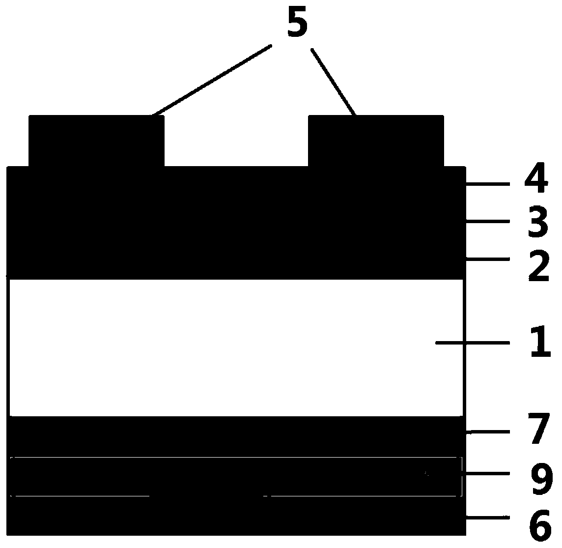
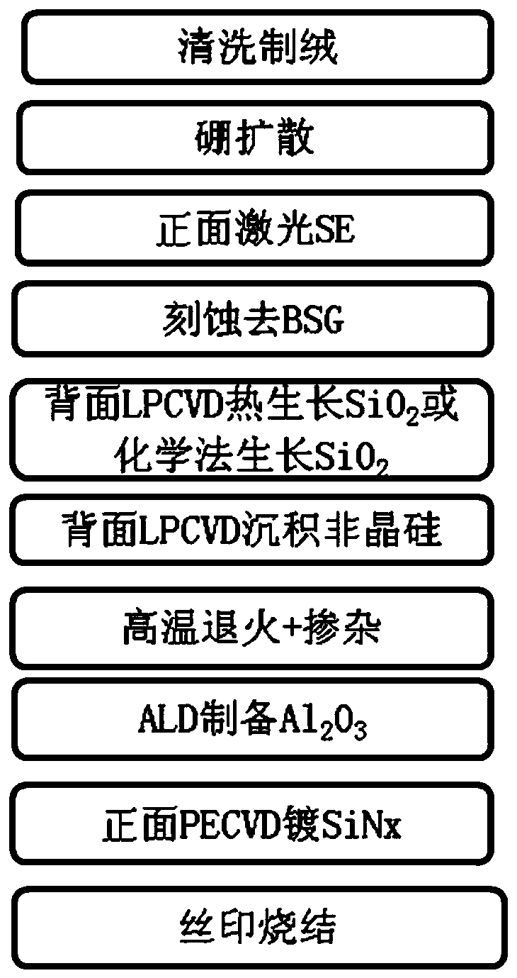
[0046] A kind of method that utilizes tubular PECVD to prepare fully passivated contact solar cell on the back, its preparation process flow chart is as follows image 3 shown, including the following steps:

[0047] (1) Pre-clean silicon wafers (specifically, N-type single crystal silicon wafers with a resistivity of 1Ω·cm~3Ω·cm) in a tank machine to remove the damaged layer, where the solution is potassium hydroxide (KOH) and hydrogen peroxide (H 2 o 2 ) mixed aqueous solution, the potassium hydroxide (KOH) and hydrogen peroxide (H 2 o 2 ) mixed aqueous solution is obtained by mixing potassium hydroxide solution and hydrogen peroxide solution, wherein the volume ratio of potassium hydroxide solution and hydrogen peroxide solution is 1:3, and the mass concentration of potassium hydroxide solution is 45%, and the mass concentration of hydrogen peroxide solution is 30%. In this step, pre-cleaning is performed at a temperature of 60° C. for 160 s.

[0048] (2) Carry out dou...

Embodiment 2

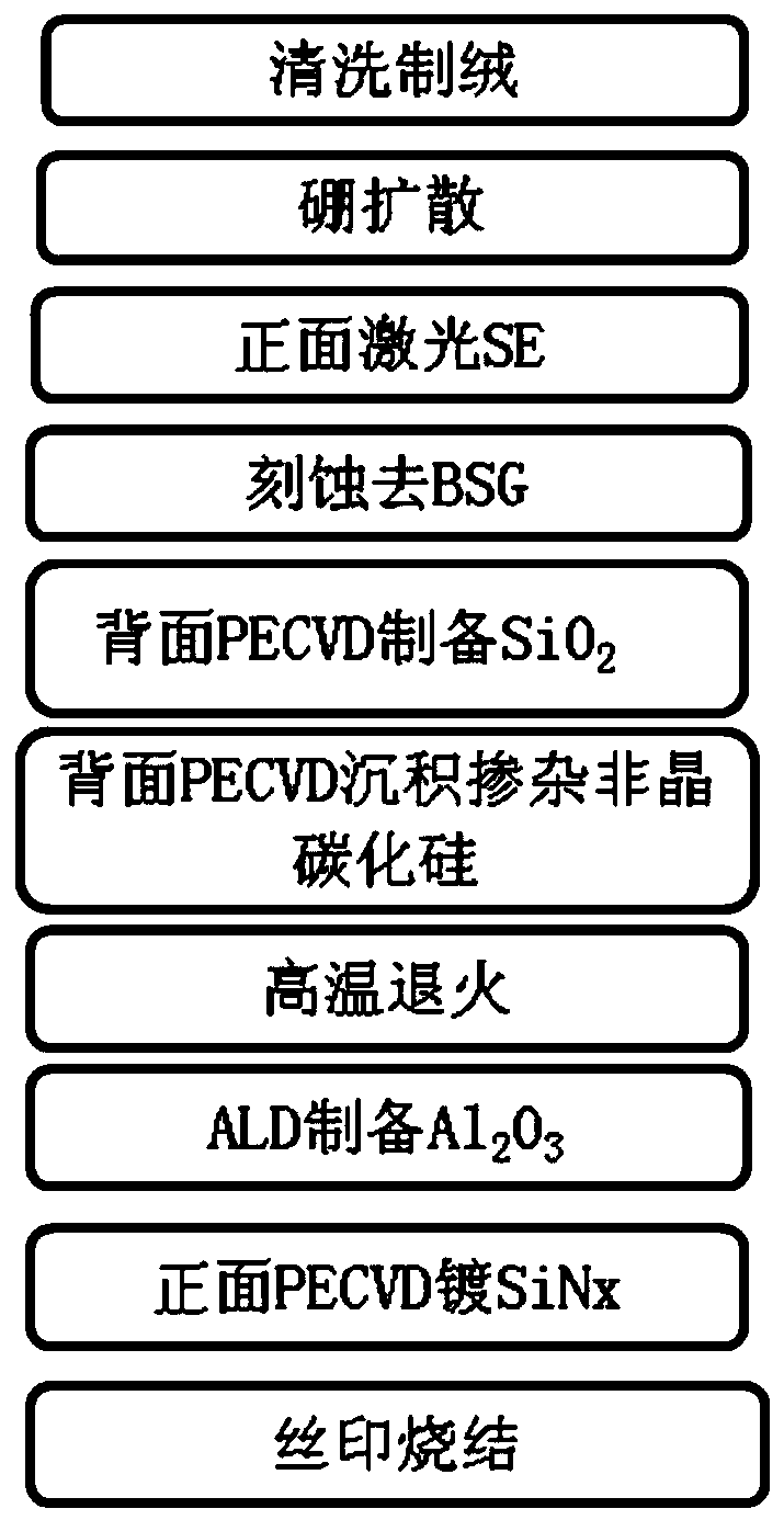
[0066] A kind of method that utilizes tubular PECVD to prepare fully passivated contact solar cell on the back side, comprises the following steps:

[0067] (1) Pre-clean silicon wafers (specifically, N-type single crystal silicon wafers with a resistivity of 1Ω·cm~3Ω·cm) in a tank machine to remove the damaged layer, where the solution is potassium hydroxide (KOH) and hydrogen peroxide (H 2 o 2 ) mixed aqueous solution, the potassium hydroxide (KOH) and hydrogen peroxide (H 2 o 2 ) mixed aqueous solution is obtained by mixing potassium hydroxide solution and hydrogen peroxide solution, wherein the volume ratio of potassium hydroxide solution and hydrogen peroxide solution is 1:3, and the mass concentration of potassium hydroxide solution is 45%, and the mass concentration of hydrogen peroxide solution is 30%. In this step, pre-cleaning is performed at a temperature of 60° C. for 160 s.

[0068] (2) double-sided texturing is carried out to the silicon chip after pre-cleani...


PUM

PropertyMeasurementUnit
electrical resistivityaaaaaaaaaa
thicknessaaaaaaaaaa
thicknessaaaaaaaaaa

Abstract

The invention discloses a method for preparing a back fully-passivated contact solar cell by utilizing tubular PECVD and the back fully-passivated contact solar cell. The method comprises the steps of carrying out pre-cleaning, double-sided texturing, front boron diffusion, front laser selective doping, secondary cleaning and back polishing on a silicon wafer; depositing a silicon dioxide thin film layer and a phosphorus-doped amorphous silicon carbide thin film layer on the back surface of the tubular PECVD equipment, and performing annealing treatment to convert amorphous silicon carbide into microcrystalline silicon carbide; depositing an Al2O3 passivation layer and an antireflection layer; and performing silk-screen printing and sintering to obtain the back fully-passivated contact solar cell. The method disclosed by the invention has the advantages of simple process, convenience in operation, low cost, good compatibility with the existing production line, good preparation controllability, high preparation efficiency, good safety and the like, can be used for preparing the high-efficiency back fully-passivated contact solar cell, is suitable for large-scale preparation, is beneficial to industrial application, and has a very high use value and a very good application prospect.

Description

technical field [0001] The invention belongs to the field of preparation of fully passivated contact solar cells on the back, and relates to a method for preparing fully passivated contact solar cells on the back by using tubular PECVD and the fully passivated contact solar cells on the back. Background technique [0002] The Tunneling Oxide / Polysilicon Passivated Contact (TOPCon) solar cell is a fully passivated contact solar cell on the back, and its structure diagram is shown in figure 1 As shown, the most important thing is the ultra-thin tunnel oxide layer and polysilicon layer, the quality of these two layers directly determines the passivation quality and battery efficiency of the battery. [0003] Currently, SiO 2 / TOPCon solar cells with fully passivated contact structure on the back of polysilicon are usually prepared by LPCVD, and the preparation process flow chart is as follows figure 2 As shown, there are the following problems: (1) Since the silicon wafers i...

Claims


Application Information

Patent Timeline
Patent Type & Authority Applications(China)
IPC IPC(8): H01L31/0216H01L31/0224H01L31/18
CPCH01L31/02168H01L31/022441H01L31/1816H01L31/1864H01L31/1868Y02E10/50Y02P70/50
Inventor 黄嘉斌赵增超周小荣周子游刘文峰
Owner HUNAN RED SUN PHOTOELECTRICITY SCI & TECH
Why Eureka
Try Eureka