

ZnO thin film structure and preparation method thereof
A technology of thin film structure and ordered structure, which is applied in the field of ZnO thin film structure and its preparation, can solve the problems of cost control, distribution uniformity and shape controllability, etc., to increase physical and chemical adsorption and expand the scope of application , performance-enhancing effects
- Summary
- Abstract
- Description
- Claims
- Application Information
AI Technical Summary
Problems solved by technology
Method used
Image

Examples
Embodiment 1
[0065] This embodiment provides a method for preparing a ZnO thin film structure, comprising the following steps:
[0066] (1) Spin-coat a 4 μm polyimide layer on a single crystal silicon substrate. During spin-coating, the rotating speed is 2500rpm, and the spin-coating time is 40s. After spin-coating, it is placed on a hot plate for baking. The baking temperature is 120℃, baking time is 10min;
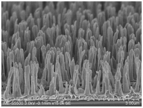
[0067] (2) Utilize plasma cleaning equipment to carry out plasma bombardment process, the plasma used is oxygen plasma and argon plasma, the flow rate of oxygen plasma gas source is 50 sccm, the flow rate of argon plasma gas source is 20 sccm, oxygen chamber The pressure is 5Pa, the argon cavity pressure is 2Pa, the radio frequency power is 350W, the oxygen plasma treatment time is 9min, and the argon plasma treatment time is 25min, and nanofibers are obtained on the substrate, such as figure 1 As shown, the diameter of the nanofiber is 50-100nm, the number of nanofibers per square ...
Embodiment 2
[0070] This embodiment provides a method for preparing a ZnO thin film structure, comprising the following steps:
[0071] (1) Spin-coat a 3 μm polyimide layer on a single crystal silicon substrate. During spin-coating, the rotating speed is 3300rpm, and the spin-coating time is 40s. After spin-coating, place it on a hot plate for baking. The temperature is 120℃, and the baking time is 10min;
[0072] (2) Utilize the plasma cleaning equipment to carry out the plasma bombardment process, the plasma used is oxygen plasma, the flow rate of the oxygen plasma gas source is 50sccm, the cavity pressure is 5Pa, the radio frequency power is 350W, and the oxygen plasma treatment time is 9min , to obtain nanofibrous structures on the substrate, such as figure 1 As shown, the diameter of the nanofiber is 100-150nm, the number of nanofibers per square micrometer is 10-15, and the height of the nanofiber is 0.85 μm;
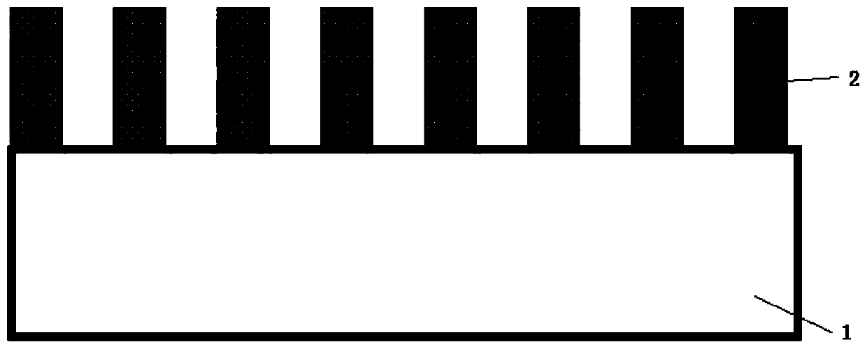
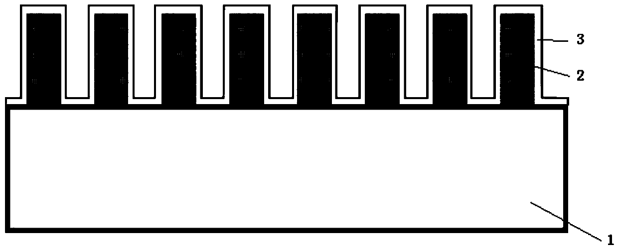
[0073] (3) Using nanofibers as a mask, reactive ion etching was perform...
Embodiment 3
[0076] The difference between this embodiment and embodiment 2 is that the parameters of each step are different, and a step of wet etching to remove nanofibers is added after step (3), to obtain a nanocone-ZnO film structure.
[0077] (1) Spin-coat a 5 μm polyimide layer on a monocrystalline silicon substrate. During spin-coating, the rotating speed is 2000rpm, and the spin-coating time is 40s. After spin-coating, place it on a hot plate for baking. The temperature is 120℃, and the baking time is 10min;
[0078] (2) Utilize the plasma cleaning equipment to carry out the plasma bombardment process, the plasma used is oxygen plasma, the flow rate of the oxygen plasma gas source is 50sccm, the cavity pressure is 5Pa, the radio frequency power is 350W, and the oxygen plasma treatment time is 9min , to obtain nanofibrous structures on the substrate, such as figure 1 As shown, the diameter of the nanofiber is 100-150nm, and the number of nanofibers in each square micron area is 10...
PUM
| Property | Measurement | Unit |
|---|---|---|
| height | aaaaa | aaaaa |
| thickness | aaaaa | aaaaa |
| diameter | aaaaa | aaaaa |
Abstract
Description
Claims
Application Information