Boron-doped diamond electrode with ultrahigh specific surface area as well as preparation method and application of boron-doped diamond electrode

An ultra-high specific surface area, diamond electrode technology, applied in the direction of electrodes, chemical instruments and methods, electrolysis process, etc., can solve the problems of slow mass transfer rate, restricting the electrocatalytic performance of BDD electrodes, and easy to fall off, so as to improve the surface roughness Effect

Active Publication Date: 2020-08-04
NANJING DAIMONTE TECH CO LTD
View PDF12 Cites 5 Cited by
  • Summary
  • Abstract
  • Description
  • Claims
  • Application Information

AI Technical Summary

Problems solved by technology

[0003] However, the BDD electrode degradation technology for organic wastewater has not been widely accepted by the market. The fundamental reasons are (1) the substrates of existing BDDs are mostly monocrystalline silicon, which is difficult to manufacture in large volumes. As the volume of monocrystalline silicon increases, , the manufacturing cost has risen sharply, which makes the existing BDD electrodes high in cost and low in cost performance, and it is difficult to fully meet the market's requirements for economical efficiency; (2) the existing BDD planar electrodes have small area, low surface roughness, and low specific surface area. The electrode has the disadvantages of small active area, low space-time yield of strong o

Method used


Image

  • Boron-doped diamond electrode with ultrahigh specific surface area as well as preparation method and application of boron-doped diamond electrode
  • Boron-doped diamond electrode with ultrahigh specific surface area as well as preparation method and application of boron-doped diamond electrode
  • Boron-doped diamond electrode with ultrahigh specific surface area as well as preparation method and application of boron-doped diamond electrode

Examples


Embodiment 1

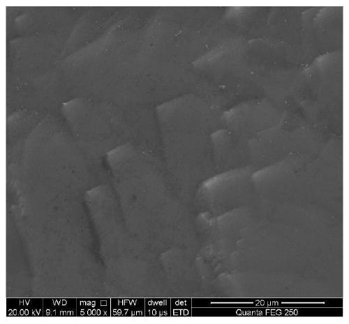
[0064] First perform anisotropic etching on the surface of the polysilicon substrate material, use 10M KOH solution as an anisotropic etching solution, place the polysilicon substrate material in the anisotropic etching solution at 80°C for 60 minutes to complete the etching, Then wash and dry to obtain step-type polysilicon with high specific surface area, whose shape is as follows figure 1 .

[0065] The etched polysilicon was placed in a suspension of nanocrystalline and microcrystalline diamond mixed particles, and ultrasonically oscillated for 30 minutes to obtain a polysilicon substrate with diamond grains attached to the surface.

[0066] Put the substrate into a chemical vapor deposition furnace, keep the distance between the hot wire and the substrate surface at 9 mm, adjust the flow rate of hydrogen gas to maintain 97 sccm during the heating process, and feed methane and borane into the furnace to start deposition. The deposition temperature is 850°C, the deposition...

Embodiment 2

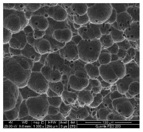
[0073] Embodiment 2 is the same as that in Embodiment 1 except that the polysilicon substrate is etched by an isotropic etching method. The surface of the polysilicon substrate material is isotropically etched first to analyze pure HF and HNO 3 The mixed solution is used as an isotropic etching solution, and the mixed volume ratio is HF:HNO 3 =3:1. The polysilicon substrate material is placed in an isotropic etching solution at room temperature for 2 minutes to complete the etching, then cleaned and dried to obtain pitted microporous composite polysilicon with a high specific surface area, and its shape is as follows: figure 2 .

[0074] The subsequent preparation process is the same as in Example 1, and the electrode properties are shown in Table 2:

[0075] The electrochemical performance of the BDD electrode gained in table 2 embodiment 2

[0076] Oxygen evolution potential / V 2.37 Hydrogen evolution potential / V -0.55 Potential window / V 2.92 B...

Embodiment 3

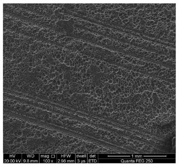
[0085] In Example 3, an anisotropic etching method is used to etch a stepped polysilicon substrate first, and then an isotropic etching method is used, and the etching parameters of the etching solution are the same as those in Embodiments 1 and 2. It looks like image 3 .

[0086] Subsequently, a BDD electrode was prepared, and the preparation method was the same as in Example 1. The electrode properties are shown in Table 4:

[0087] The electrochemical performance of the BDD electrode gained in table 4 embodiment 3

[0088] Oxygen evolution potential / V 2.52 Hydrogen evolution potential / V -0.63 Potential window / V 3.15 Background current / μA / cm 2

12.62

[0089] It can be seen from the above data that the combination of anisotropic etching method and isotropic etching method to etch polysilicon substrate has excellent electrochemical performance and good reversibility of the electrode.

[0090] The BDD electrode prepared in embodiment 3 ...


PUM


Abstract

The invention discloses a boron-doped diamond electrode with an ultrahigh specific surface area as well as a preparation method and application of the boron-doped diamond electrode. The boron-doped diamond electrode comprises a substrate and an electrode working layer, wherein the electrode working layer is wrapped on the surface of the substrate, and the substrate is polycrystalline silicon or monocrystalline silicon with a high specific surface area; the electrode working layer is a boron-doped diamond layer; the polycrystalline silicon with the high specific surface area is obtained by performing anisotropic etching or/and isotropic etching on the surface of the polycrystalline silicon; and the monocrystalline silicon with the high specific surface area is obtained by performing anisotropic etching on the surface of the monocrystalline silicon. The boron-doped diamond electrode is characterized in that the boron-doped diamond layer comprises a boron-doped diamond high-conductivity layer, a boron-doped diamond corrosion-resistant layer and a boron-doped diamond strong electrocatalytic activity layer which are different in boron content, and compared with a traditional plate electrode, the silicon-based boron-doped diamond electrode has the advantages of being low in cost and extremely high in specific surface area, and relatively high current intensity is provided by using relatively low current density, so that the a wide application prospect is provided.

Description

technical field [0001] The invention discloses a super-high specific surface area boron-doped diamond electrode and its preparation method and application, belonging to the technical field of surface etching modification and vapor deposition. Background technique [0002] Boron-doped diamond film electrode (BDD) has high mechanical strength, chemical inertness and excellent electrochemical performance, such as a wide potential window in aqueous solution, high oxygen evolution overpotential and low background current, Hydroxyl radicals can be generated efficiently at the same current density, so that organic matter can be quickly removed, the surface has anti-poisoning and anti-pollution capabilities, and can work stably for a long time in strong corrosive media. Even under high electrochemical load, the passing current density is 2~10A cm 2 After thousands of hours of electrochemical reaction, there is no obvious sign of corrosion. The diamond film has high quality propert...

Claims


Application Information

Patent Timeline
IPC IPC(8): C23C16/27C23C16/56C23C16/02C25B11/06C25B1/13C02F1/461C02F1/72
CPCC23C16/278C23C16/277C23C16/56C23C16/0227C25B1/13C02F1/4672C02F1/46109C02F2001/46138C25B11/059C25B11/051C25B11/091C02F2001/46147C25B11/052C25B11/083C23C16/0272C23C16/271C02F2303/04
Inventor 魏秋平马莉周科朝王立峰王宝峰施海平
Owner NANJING DAIMONTE TECH CO LTD
Why Eureka
Try Eureka