Preparation method of gallium oxide film based on Zn and N co-doping

A thin-film preparation and gallium oxide technology, which is applied in semiconductor/solid-state device manufacturing, electrical components, circuits, etc., can solve the problems of introduction, reduction of p-type gallium oxide hole carrier mobility, deep impurity energy level, etc. Achieve high chemical stability, reduce impurity formation energy, and good p-type characteristics

Pending Publication Date: 2020-10-13
XIDIAN UNIV
View PDF1 Cites 0 Cited by
  • Summary
  • Abstract
  • Description
  • Claims
  • Application Information

AI Technical Summary

Problems solved by technology

However, the shortcomings of this film are that the position of the introduced impurity level is relatively deep, and it will introduce background donor concentration, resulting in a decrease in the mobility of p-type gallium oxide holes.

Method used


Image

  • Preparation method of gallium oxide film based on Zn and N co-doping
  • Preparation method of gallium oxide film based on Zn and N co-doping
  • Preparation method of gallium oxide film based on Zn and N co-doping

Examples


Embodiment 1

[0025] Example 1: Preparation of a gallium oxide thin film with sapphire as a substrate and Zn and N doping concentrations of 0.125 and 0.083, respectively.

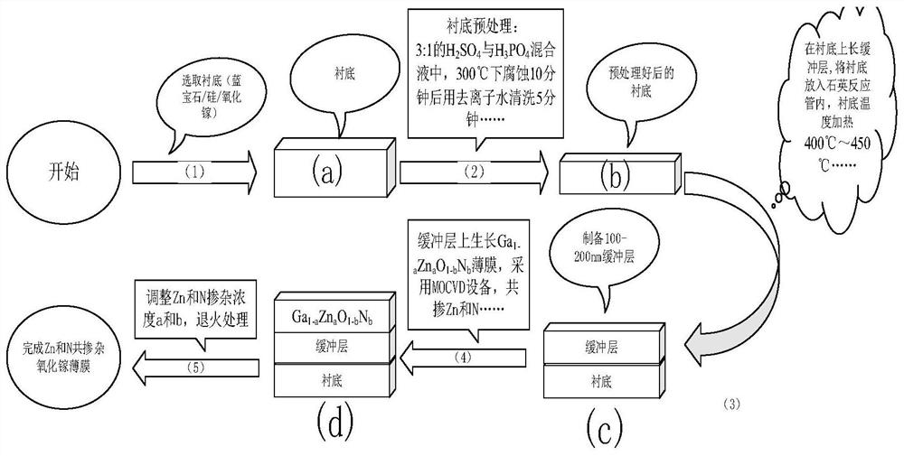
[0026] Step 1: Choose sapphire as the substrate, such as figure 1 (a).

[0027] In the second step, the sapphire substrate is pretreated for cleaning and etching.

[0028] 2.1) The sapphire substrate was ultrasonically cleaned in acetone for 10 minutes, then the substrate was ultrasonically cleaned in absolute ethanol for 10 minutes, and then rinsed repeatedly with deionized water for 3 times; then it was placed in 3:1 H 2 SO 4 with H 3 PO 4 In the mixed solution, corrode at 300°C for 10 minutes and then wash with deionized water for 5 minutes;

[0029] 2.2) heat-treat the cleaned substrate at a temperature of 1380° C. in a hydrogen H2 atmosphere for 1 hour to obtain a pretreated sapphire substrate, such as figure 1 (b).

[0030] Step 3: Grow 150nm thick Ga on sapphire substrate 2 o 3 The buffer layer.

[0031]...

Embodiment 2

[0040] Example 2: Preparation of gallium oxide thin films with 6H-SiC substrate and Zn and N doping concentrations of 0.0417 and 0.0625, respectively.

[0041] Step 1: Select 6H-SiC as the substrate.

[0042] Step 2: Perform cleaning and etching pretreatment on the 6H-SiC substrate.

[0043] The specific realization of this step is the same as that of the second step of Embodiment 1.

[0044] Step 3: Grow 100nm thick Ga on 6H-SiC substrate 2 o 3 The buffer layer.

[0045] Put the pretreated substrate into the reaction chamber first, turn on the vacuum pump to evacuate the reaction chamber to 10 -2 Pa. Using Ga(C 2 h 5 ) 3 and O 2 As Ga source and O source respectively, the temperature of the source bottle is maintained at -10°C to 20°C through a semiconductor cold trap, the inert gas Ar is used as the carrier gas, and high-purity He is used as the auxiliary gas flow;

[0046] Then heat the substrate, stop for 1min every time the temperature rises by 50°C, and heat th...

Embodiment 3

[0053] Embodiment 3: Prepare a gallium oxide thin film with a gallium oxide substrate, and the doping concentrations of Zn and N are 0.031 and 0.021, respectively.

[0054] Step A: Gallium oxide is selected as the substrate.

[0055] Step B: performing cleaning and etching pretreatment on the gallium oxide substrate.

[0056] The specific realization of this step is the same as that of the second step of Embodiment 1.

[0057] Step C: Grow 200nm thick Ga 2 o 3 The buffer layer.

[0058] C1) Put the pretreated substrate into the reaction chamber, turn on the vacuum pump to evacuate the reaction chamber to 5×10 -3 Pa. Using Ga(C 2 h 5 ) 3 and O 2 As Ga source and O source respectively, the temperature of the source bottle is maintained at -10°C to 20°C through a semiconductor cold trap, the inert gas Ar is used as the carrier gas, and high-purity He is used as the auxiliary gas flow;

[0059] C2) Heating the substrate, stopping for 1 minute every time the temperature r...


PUM


Abstract

The invention discloses a preparation method of a gallium oxide film based on Zn and N co-doping, and mainly solves the problems of low hole concentration and higher acceptor level position of the existing p-type doped gallium oxide. According to the implementation scheme, the method comprises the following steps: 1) selecting a substrate and carrying out cleaning and corrosion pretreatment on thesubstrate; 2) preparing a buffer layer with the thickness of 100nm-200nm on the pretreated substrate by adopting a metal organic chemical vapor deposition process; and 3) respectively controlling thedoping concentration a of Zn to be 0.031 to 0.125 and the doping concentration b of N to be 0.021 to 0.083 on the prepared buffer layer, and growing the Zn and N co-doped Ga1-aZnaO1-bNb film. According to the invention, the peak value of the state density near the Fermi level of the film is improved, the impurity formation energy of the film is reduced, the film has higher chemical stability, theacceptor level is closer to the top of a valence band, better migration characteristics are shown, and the film can be used for manufacturing semiconductor light-emitting devices.

Description

technical field [0001] The invention belongs to the technical field of semiconductor materials, and further relates to a preparation method of gallium oxide thin film, which can be used to manufacture semiconductor light-emitting devices. Background technique [0002] With the rapid development of information technology in modern society, represented by semiconductor technology, people's demand for high withstand voltage, low power consumption electronic devices and high temperature resistant, radiation resistant deep ultraviolet light devices is increasing day by day. After years of development, the performance of the third-generation wide-bandgap semiconductor materials and devices represented by GaN and SiC has gradually approached or even exceeded that of silicon-based power devices. However, the development of industrial applications of semiconductor materials such as GaN and SiC is limited because of the difficulty and high cost of their preparation. Therefore, it is ...

Claims


Application Information

Patent Timeline
IPC IPC(8): H01L21/02H01L31/0224H01L33/42
CPCH01L21/02483H01L21/02565H01L21/0257H01L21/0262H01L31/022466H01L33/42
Inventor 苏杰常晶晶严崇勇林珍华郝跃
Owner XIDIAN UNIV
Why Eureka
Try Eureka