Method for reducing thickness of tellurium nanosheet

A technology of thickness reduction and tellurium nanometer, applied in the field of nanomaterials, can solve the problems of complex process, complicated operation method, poor sample thinning effect, etc., and achieve the effect of stable development performance, simple operation and good compatibility.

Active Publication Date: 2021-09-17
UNIV OF SCI & TECH BEIJING
View PDF4 Cites 1 Cited by
  • Summary
  • Abstract
  • Description
  • Claims
  • Application Information

AI Technical Summary

Problems solved by technology

However, the effect of this method to thin the sample is poor, and the operation method is complicated
People such as Javey have obtained a thickness-controllable tellurium nanofilm by low-temperature thermal evaporation, but when evaporating a very thin nanofilm (8nm), the impact of impurities, crystal quality and surface roughness becomes very large (Nat. Nanotechnol. 15, 53–58 (2020))
These methods generally have the disadvantages of complicated process and great damage to the surface morphology of samples.

Method used


Image

  • Method for reducing thickness of tellurium nanosheet
  • Method for reducing thickness of tellurium nanosheet
  • Method for reducing thickness of tellurium nanosheet

Examples


Embodiment 1

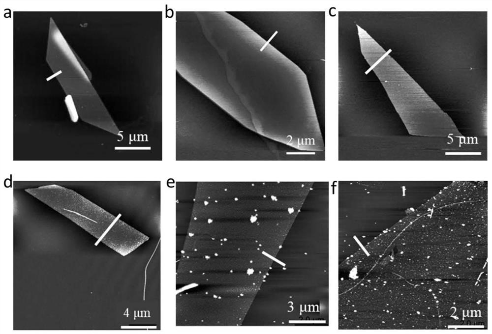
[0035](1) Preparation of tellurium nanosheets by hydrothermal method: the reaction principle is to use sodium tellurite as raw material, ammonia water provides the alkaline conditions for the reaction, hydrazine hydrate is used to reduce sodium tellurite, and the mirror blocking ligand (PVP) is used to reunite Tellurium nanoparticles, by controlling the amount of PVP added to control the output and size of tellurium nanosheets. The specific operation is to weigh 0.1165g of sodium tellurite and 6.4g of PVP in a molar ratio of 2:1 and dissolve them in 25ml of deionized water. 9, pour the mixed solution into a 50ml reaction kettle, and react at 180°C for 10 hours. After the reaction, quench the reaction kettle with flowing cold water to obtain the stock solution of tellurium nanosheets; take 3 mL of the reaction stock solution and centrifuge it with deionized water for 3 After the second step, uniformly dispersed tellurium nanosheets in the aqueous solution were obtained, and the...

Embodiment 2

[0041] (1) The preparation method of tellurium nanosheets is the same as step (1) of Example 1, the difference is that the specific operation is to weigh 0.1165g of sodium tellurite and 6.4g of PVP in 25ml of deionized water in a molar ratio of 2:1, and stir After uniformity, add 2.5ml of ammonia water and 4ml of hydrazine hydrate solution and stir evenly, pour the mixed solution into a 50ml reaction kettle, and react at 180°C for 5h. After the reaction, quench the reaction kettle with flowing cold water to obtain tellurium nanosheets Stock solution: Take 3 mL of the reaction stock solution and centrifuge it with deionized water for 3 times to obtain tellurium nanosheets uniformly dispersed in the aqueous solution. Transfer the tellurium nanosheets to an insulating silicon substrate by pulling and pulling method, and dry them naturally at 100°C for 20 minutes. , the thickness of the obtained tellurium nanosheets is 30-50nm.

[0042] (2) Slow thinning of tellurium nanosheets: i...

Embodiment 3

[0045] (1) The preparation method of tellurium nanoplate is the same as embodiment 2 step (1);

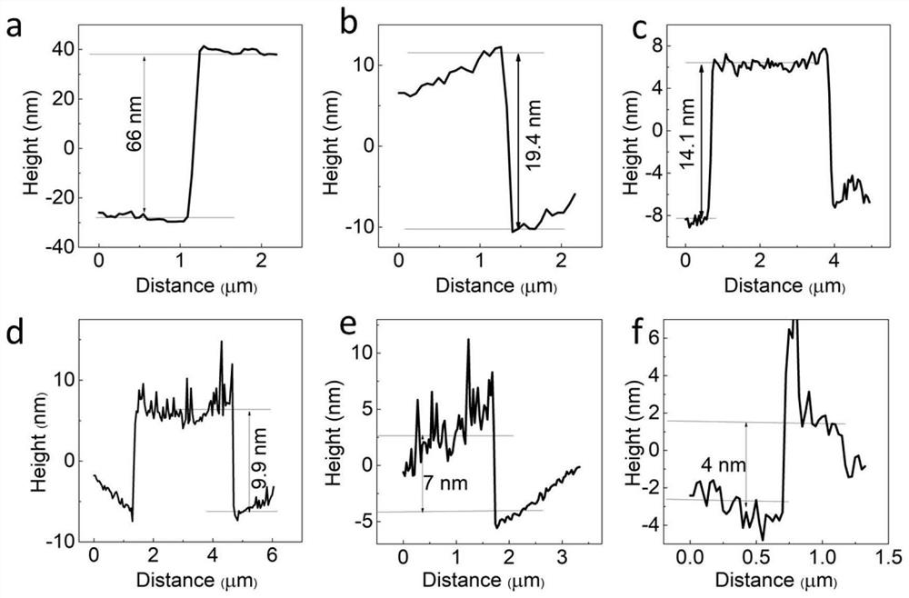
[0046] (2) Slow thinning of tellurium nanosheets: immerse the tellurium nanosheets on the insulating silicon substrate obtained in step (1) into an acetic acid solution with a pH of 6 for 20 s. The tellurium nanosheets were soaked in the acetic acid solution for 20s, then quickly taken out and washed with a large amount of deionized water, and then dried with nitrogen to obtain a thin layer of tellurium nanosheets with a single layer to 25nm.

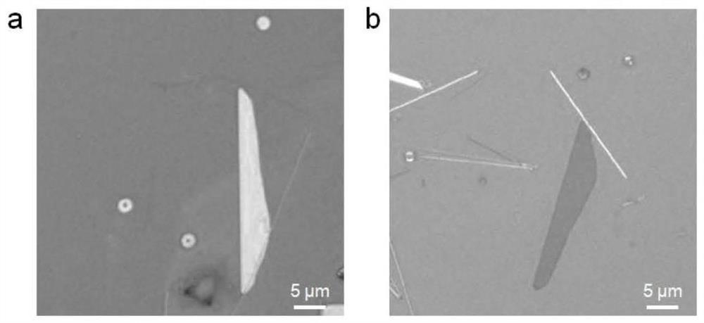
[0047] In order to better compare the morphology changes of the tellurium nanosheets before and after immersion in the acetic acid solution with pH 6, the same piece of tellurium nanosheets was selected for comparison. Figure 5 a, 5b are the AFM morphology characterization of the samples before and after immersion in acetic acid solution with pH 6 for 20s. It can be seen that the morphology of tellurium nanosheets has no obvious change befo...


PUM

PropertyMeasurementUnit
sizeaaaaaaaaaa
thicknessaaaaaaaaaa
thicknessaaaaaaaaaa

Abstract

The invention discloses a method for reducing the thickness of a tellurium nanosheet, and belongs to the technical field of nano materials, the method comprises the following steps: soaking the tellurium nanosheet in a weak oxidizing solution, taking out and drying to obtain the tellurium nanosheet with the reduced thickness, according to the method, the weak oxidizing solution and the surface of the tellurium nanosheet are subjected to mild oxidation reaction, the tellurium nanosheet is thinned, and accurate regulation and control of the thickness of the tellurium nanosheet can be achieved; according to the thin-layer tellurium nanosheet prepared by the method disclosed by the invention, the advantages of the p-type tellurium nanosheet can be fully played, the requirements of different devices on material performance are met, electronic and photoelectric devices based on the tellurium nanosheet can be constructed by utilizing electron beam exposure and vacuum evaporation of an electrode material, and the thin-layer tellurium nanosheet has good compatibility with a traditional semiconductor processing technology; according to the invention, multiple regulation and control of the thickness, the carrier concentration and the field effect switching ratio of the tellurium nanosheet can be realized, and support is provided for developing a two-dimensional p-type semiconductor material which is stable in performance and meets multi-scene requirements.

Description

technical field [0001] The invention belongs to the technical field of nanometer materials, and in particular relates to a method for reducing the thickness of tellurium nanosheets. Background technique [0002] For more than half a century, Moore's Law has driven the silicon electronics industry toward smaller and faster transistors. However, the size of the silicon-based CMOS process is getting closer to the Moore limit, and at the same time, the power consumption problem caused by the size reduction is getting more and more serious. The semiconductor industry urgently needs to find new materials and new principle devices to further enhance the next generation of information processing technology. Two-dimensional materials have the advantages of high mobility, adjustable bandgap, large specific surface area, and atomic-level thickness, which can avoid the problems of transistor performance degradation and power consumption increase caused by short-channel effects. It is th...

Claims


Application Information

Patent Timeline
Patent Type & Authority Applications(China)
IPC IPC(8): C01B19/02B82Y40/00
CPCC01B19/02B82Y40/00
Inventor 张跃于慧慧张铮曾浩然张先坤高丽洪孟羽汤文辉李瑞山卫孝福
Owner UNIV OF SCI & TECH BEIJING
Why Eureka
Try Eureka