PIN diode based on n-type gallium oxide and p-type diamond and preparation method thereof

A technology of PIN diode and gallium oxide, which is applied in the field of PIN diode and its preparation, can solve the problems of obvious thermal effect, large reverse leakage current, low diode reverse bias voltage, etc., and achieve high carrier mobility and wide bandgap width , On-resistance reduction effect

Pending Publication Date: 2022-07-29
XIDIAN UNIV
View PDF0 Cites 0 Cited by
  • Summary
  • Abstract
  • Description
  • Claims
  • Application Information

AI Technical Summary

Problems solved by technology

[0005] In order to improve the problems of gallium oxide-based Schottky barrier diodes with low reverse bias voltage, large reverse leakage current, and obvious thermal effect, the invention provides a PIN diode based on n-type gallium oxide-p-type diamond and its preparation method

Method used


Image

  • PIN diode based on n-type gallium oxide and p-type diamond and preparation method thereof
  • PIN diode based on n-type gallium oxide and p-type diamond and preparation method thereof
  • PIN diode based on n-type gallium oxide and p-type diamond and preparation method thereof

Examples


Embodiment 1

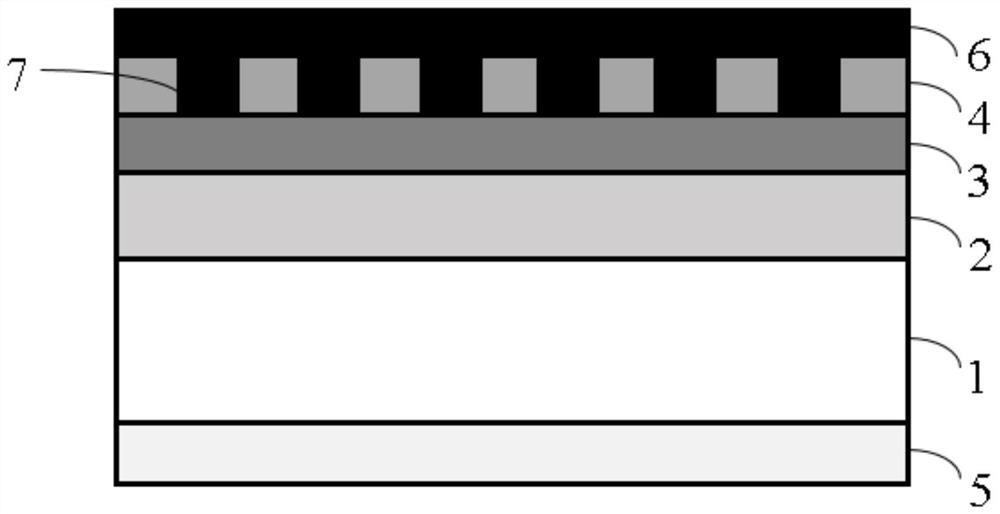
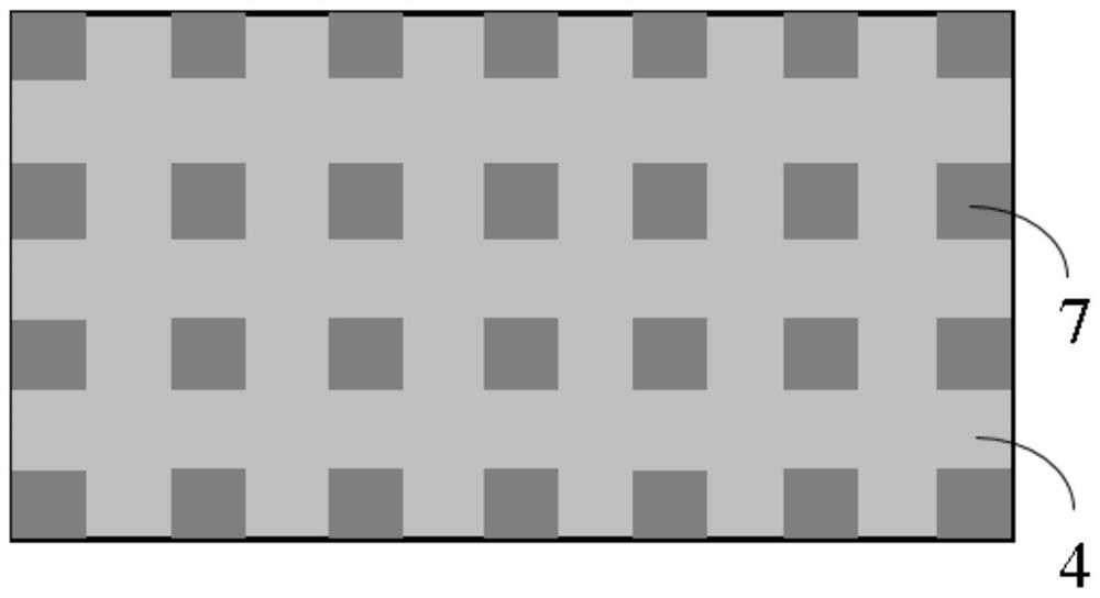
[0040] See figure 1 , figure 1 It is a schematic structural diagram of a PIN diode based on n-type gallium oxide and p-type diamond provided by an embodiment of the present invention. The PIN diode includes n + -Ga 2 O 3 Substrate layer 1, n - -Ga 2 O 3 Layer 2, p + Type diamond layer 3, p ++ type diamond layer 4, cathode layer 5 and anode layer 6, wherein the cathode layer 5, n + -Ga 2 O 3 Substrate layer 1, n - -Ga 2 O 3 layer 2 and p + The diamond layers 3 are arranged in sequence from bottom to top, p ++ The p+-type diamond layer 4 is arranged on the upper surface of the p+-type diamond layer 3 .

[0041] Further, n - -Ga 2 O 3 The doping concentration of layer 2 is less than n + -Ga 2 O 3 Doping concentration of substrate layer 1 . The substrate selected in this embodiment is heavily doped n-type gallium oxide (n + -Ga 2 O 3 ) substrate, n + -Ga 2 O 3 The doping concentration of the substrate layer 1 is 10 18 ~10 20 cm -3 , the thickness is...

Embodiment 2

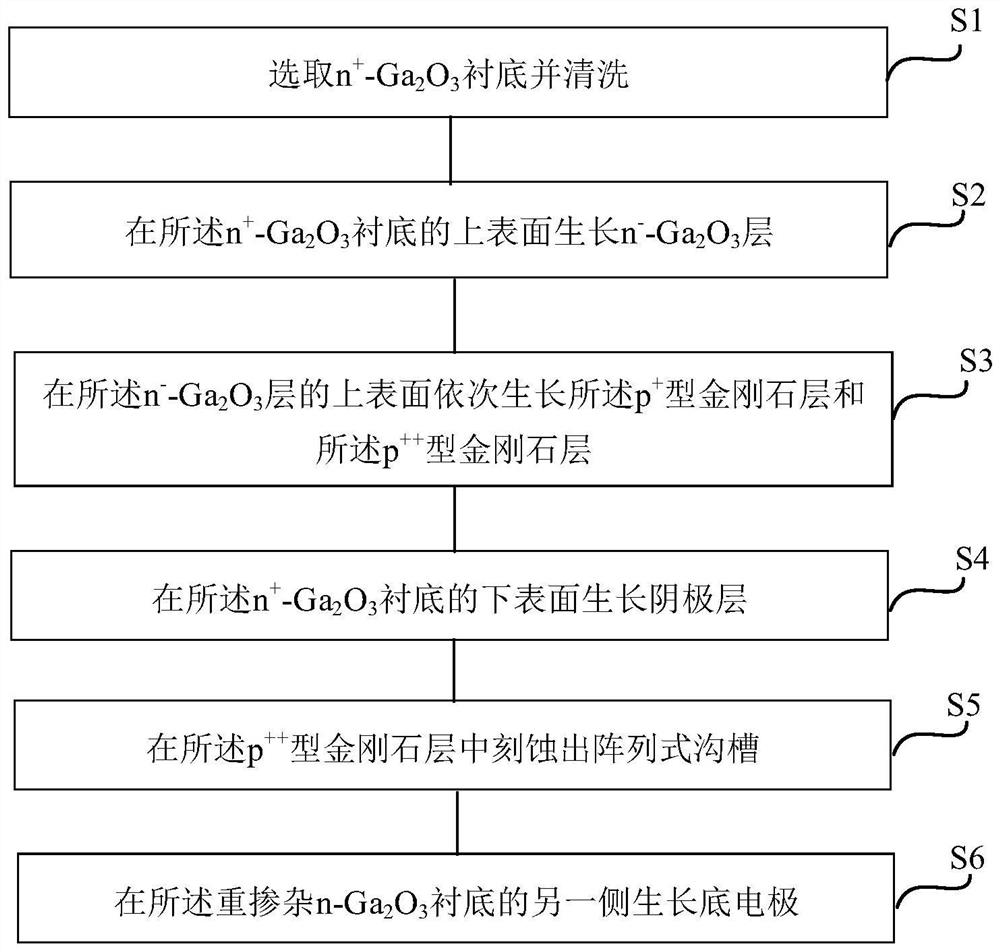
[0048] On the basis of Embodiment 1, this embodiment provides a preparation method of a PIN diode based on n-type gallium oxide and p-type diamond. See image 3 , image 3 It is a flow chart of a preparation method of a PIN diode based on n-type gallium oxide and p-type diamond provided by the embodiment of the present invention, and the preparation method includes:

[0049] S1: choose n + -Ga 2 O 3 Substrate 1 and cleaned.

[0050] Specifically, the doping concentration is selected as 1018 ~10 20 cm -3 , heavily doped n-type gallium oxide (n + -Ga 2 O 3 ) Substrate 1 and standard cleaning.

[0051] S2: at the n + -Ga 2 O 3 The upper surface of substrate 1 grows n - -Ga 2 O 3 layer 2, and the n - -Ga 2 O 3 The doping concentration of the layer is less than the n + -Ga 2 O 3 Doping concentration of the substrate layer.

[0052] Specifically, using a metal organic chemical vapor deposition (MOCVD) process or a hydride vapor phase epitaxy (HVPE) process, th...


PUM

PropertyMeasurementUnit
thicknessaaaaaaaaaa
thicknessaaaaaaaaaa
thicknessaaaaaaaaaa

Abstract

The invention discloses a PIN diode based on n-type gallium oxide and p-type diamond, which comprises an n +-Ga2O3 substrate layer, an n-Ga2O3 layer, a p + type diamond layer, a p + + type diamond layer, a cathode layer and an anode layer, and is characterized in that the cathode layer, the n +-Ga2O3 substrate layer, the n-Ga2O3 layer and the p + type diamond layer are sequentially arranged from bottom to top, the p + + type diamond layer is arranged on the upper surface of the p + type diamond layer, a plurality of grooves are formed in the p + + type diamond layer, and the anode layer covers the interiors of the grooves and the upper surface of the p + + type diamond layer; the doping concentration of the n-Ga2O3 layer is smaller than the doping concentration of the n +-Ga2O3 substrate layer, and the doping concentration of the p + + type diamond layer is larger than the doping concentration of the p + type diamond layer. According to the PIN diode structure based on the n-type gallium oxide and the p-type diamond, the voltage resistance of the PIN diode can be enhanced, the on resistance is reduced, the reverse leakage current is reduced, the heat conduction performance is improved, and the reliability of a device is improved.

Description

technical field [0001] The invention belongs to the technical field of semiconductor devices, in particular to a PIN diode based on n-type gallium oxide and p-type diamond and a preparation method thereof. Background technique [0002] In order to prepare radiation-resistant high-density, high-power optoelectronic devices, the field of semiconductor device research and preparation has gradually changed from the first generation of semiconductors to include silicon carbide (SiC), zinc oxide (ZnO), gallium oxide (Ga 2 O 3 ) and third-generation semiconductor materials such as diamond, and play a key role in the fields of new energy, smart grids, automobiles, high-speed transportation and aerospace. As an ideal semiconductor device, it is required to have excellent static and dynamic characteristics, can withstand high voltage in the blocking state, have high current density and low on-state voltage drop in the on-state, and can withstand high voltage in the on-state and on-st...

Claims


Application Information

Patent Timeline
Patent Type & Authority Applications(China)
IPC IPC(8): H01L29/868H01L29/267H01L23/373H01L29/45H01L21/329
CPCH01L29/868H01L29/267H01L23/3738H01L29/45H01L29/6603
Inventor 马晓华侯斌常青原杨凌张濛武玫郝跃
Owner XIDIAN UNIV
Why Eureka
Try Eureka