Method and device for light etching micrometer structure of smooth surface

A technology with smooth surface and microstructure, applied in microlithography exposure equipment, photolithographic process exposure devices, electrical components, etc., can solve the problems of short beam coherence length, limited processing accuracy, low absorption rate, etc. , the effect of reducing the area, high performance and price ratio

Active Publication Date: 2006-08-23
苏州迈塔光电科技有限公司 +2
View PDF0 Cites 20 Cited by
  • Summary
  • Abstract
  • Description
  • Claims
  • Application Information

AI Technical Summary

Problems solved by technology

[0007] (1) In order to obtain a high-energy-density light spot, high energy density is mainly formed by focusing a single beam. When the pulsed laser with a wavelength of 1060nm and 532nm processes the surface of a material (such as a metal), the material has a low absorption rate of light and the thermal effect is very obvious. During processing, the material is ablated by locally generating high temperature, and a large amount of light energy is converted into heat energy, forming a crater effect; thus, the minimum light spot is generally around 30-50 μm, which cannot be focused into a thinner beam, and th

Method used


Image

  • Method and device for light etching micrometer structure of smooth surface
  • Method and device for light etching micrometer structure of smooth surface
  • Method and device for light etching micrometer structure of smooth surface

Examples


Embodiment 1

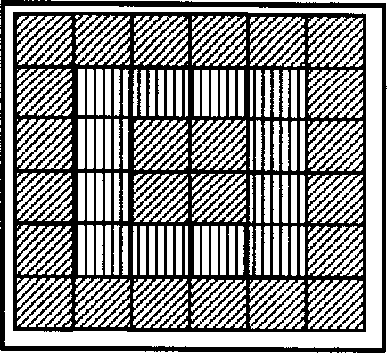
[0061] Embodiment one: see attached figure 2 As shown, a grating image production method converts the image distribution into a pulse control signal. According to the orientation and space frequency of the unit grating, the interference optical head, platform movement, high-speed grating rotation, and optical pulse input are performed at the same time. Continuous exposure on the recording material, the platform, optical head, and beam splitting elements do not need to pause during exposure until the entire image is produced. See the attached Figure 4 .

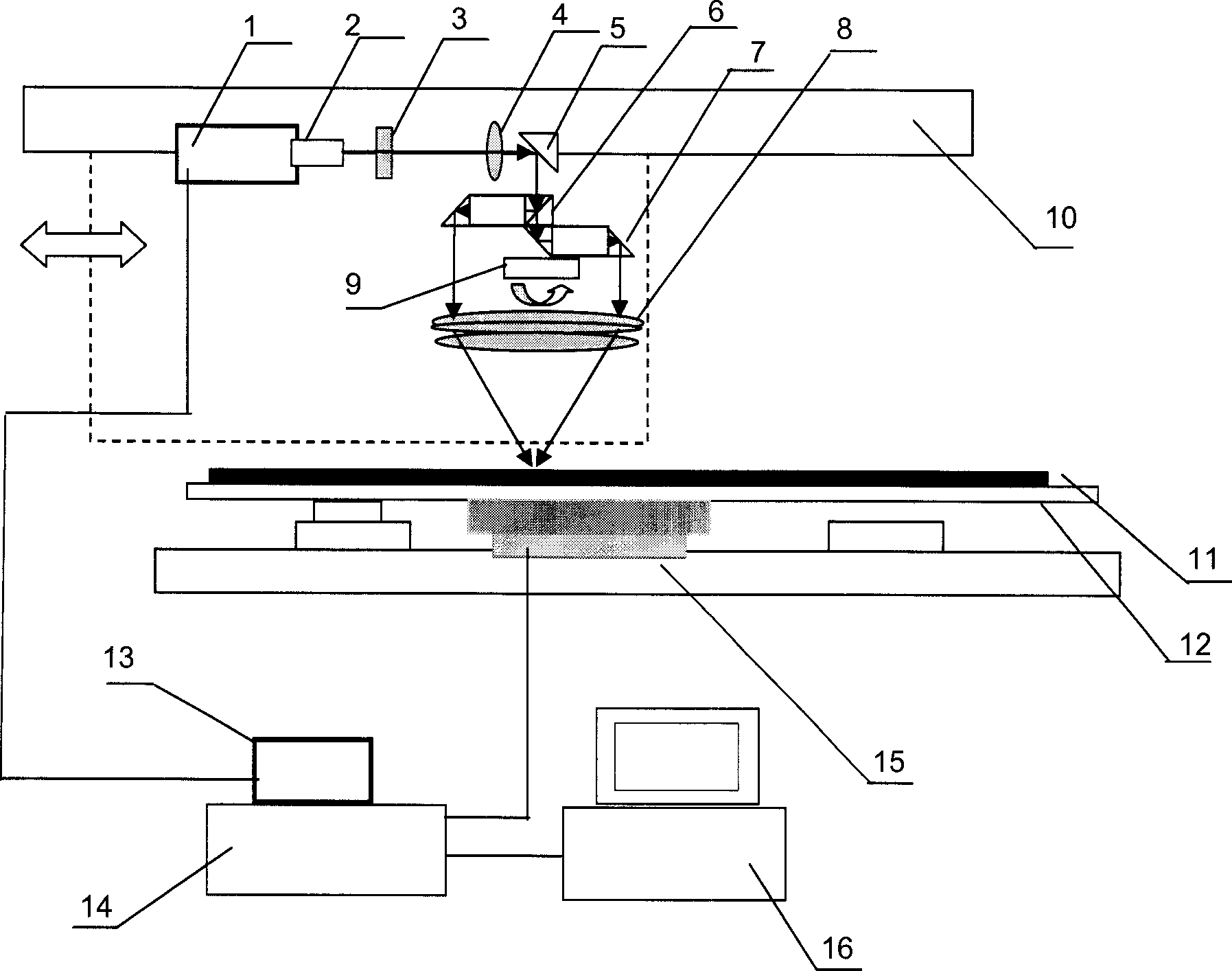
[0062]The laser lithography direct writing system that realizes the above method includes a DPSSL laser light source 1 output by ultraviolet light with a TTL signal interface, a beam expander collimator mirror 2, an iris diaphragm 3, a quartz lens 4 (objective lens), and a reflector 5 It forms a 4F system together with the quartz lens group 8, and forms a reduced image on the surface of the recording material 11 for the re...

Embodiment 2

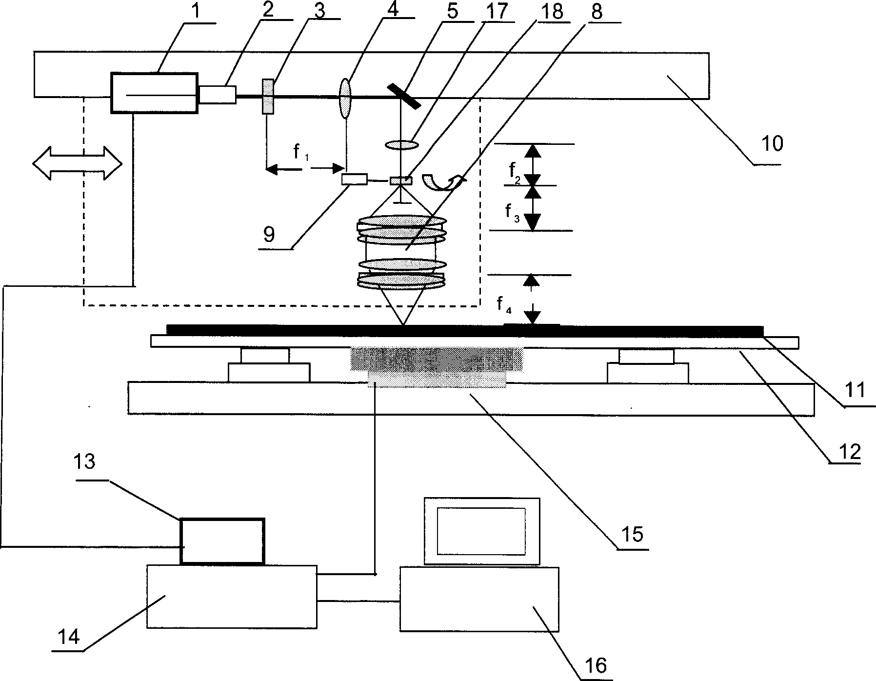
[0065] Embodiment two: see attached image 3 As shown, a photolithography system for making grating images, including laser light source 1, beam expander and collimator mirror 2, variable rectangular diaphragm 3, beam shaping system 4, 5, 17 (lenses f1, f2 The 4F system with the aperture constitutes a miniature function), the beam splitting system (including the beam splitting element quartz phase grating 18, the imaging lens group 8, the high-speed turntable 9), the above-mentioned interference optical The head is assembled on the system 10 of horizontal movement (X direction), the recording material 11 is placed on the working platform 12 (Y direction movement), and the power supply 13 including TTL and power control, the motion system control system 14, 15 and the computer 16.

[0066] The light source 1 can be a pulsed laser light source with ultraviolet output; the rectangular diaphragm can be adjusted. The spectroscopic element is placed on the turntable, and the turnta...

Embodiment 3

[0067] Embodiment 3: A method for making a grating image. First, the image is decomposed into different sub-images according to the orientation of the interference fringes, and each sub-image is continuously exposed. During the exposure of the sub-images, the beam splitting element in the optical head There is no need to rotate, only the beam splitting element is rotated when switching sub-images. This manufacturing method avoids large-angle rotation during continuous operation, and improves the continuity of photolithography operation and the quality of grating image production. See attached Figure 5 .

[0068] The overall structure of the photolithography system in this embodiment is the same as that in Embodiment 1.


PUM

PropertyMeasurementUnit
Etching depthaaaaaaaaaa

Abstract

This invention discloses a method for photo-etching smooth surfaces, which takes a large power laser as the light source, collimates the laser beams to parallel lights to pass through diaphragms and a lens to generate split light beams by a splitting element to be gathered on a material surface to form a uniform interference fringe optical field then carries out photo-etching exceeding the material harmful threshold value on the surface of the smooth material characterizing that three or four multiplications of a large power solid laser pumped by diode output by ultraviolet rays are applied as the light source, said diaphragm is an adjustable rectangle and single time pulse process is done at a same position to control the power of the laser so that the material of the interference fringe light-intensity additive position is gasified to form a fringe structure on the surface of the material and mum-stage fringe high speed laser system is realized by this method.

Description

technical field [0001] The invention relates to the processing of a hard smooth surface, in particular to a method for forming a micron-scale grating image on a smooth surface by laser etching, and a high-speed laser photoetching device for realizing the method. Background technique [0002] In order to adapt to the industrialization of high-tech in the 21st century and meet the needs of micro-manufacturing, it is imperative to research and develop high-performance advanced laser processing technology. As a branch of laser processing, laser micromachining has been widely concerned in the past ten years. As one of the unit micromachining technologies in the microelectronics integration process, it has now formed a fixed model and has been put into large-scale production. Laser wavelengths range from far infrared to X-rays, and are currently mainly used in the three major fields of microelectronics, micromechanics and micro-optical processing. Due to...

Claims


Application Information

Patent Timeline
IPC IPC(8): G03F7/20H01L21/027
Inventor 陈林森魏国军周小红解正东浦东林吴建宏解剑锋沈雁汪振华
Owner 苏州迈塔光电科技有限公司
Why Eureka
Try Eureka