Metal silicide nano-wire and its making method

A technology of metal silicide and a manufacturing method, which is applied in the fields of semiconductor/solid-state device manufacturing, electrical components, electrical solid-state devices, etc., can solve the problems of disordered metal silicide nanowires, difficult to control size and shape, uncontrollable growth position, etc. Achieve the effect of improving characteristics and reliability, small line width and high efficiency

Inactive Publication Date: 2007-06-13
INST OF PHYSICS - CHINESE ACAD OF SCI
View PDF0 Cites 26 Cited by
  • Summary
  • Abstract
  • Description
  • Claims
  • Application Information

AI Technical Summary

Problems solved by technology

[0006] The purpose of the present invention is to not only overcome the defect that the size and shape of the existing method for preparing metal silicide nanowires are not easy to control; ; Thereby providing a metal silicide nanowire manufacturing method with controllable size, shape and growth position and the prepared metal silicide nanowire, and can be used for interconnection wires and electrodes of integrated circuits, and can also be used for researching nanowires Relationship between Physical and Chemical Properties and Linewidth and Direct Fabrication of Nanoelectronic Devices and Circuits

Method used


Image

  • Metal silicide nano-wire and its making method
  • Metal silicide nano-wire and its making method

Examples


Embodiment 1

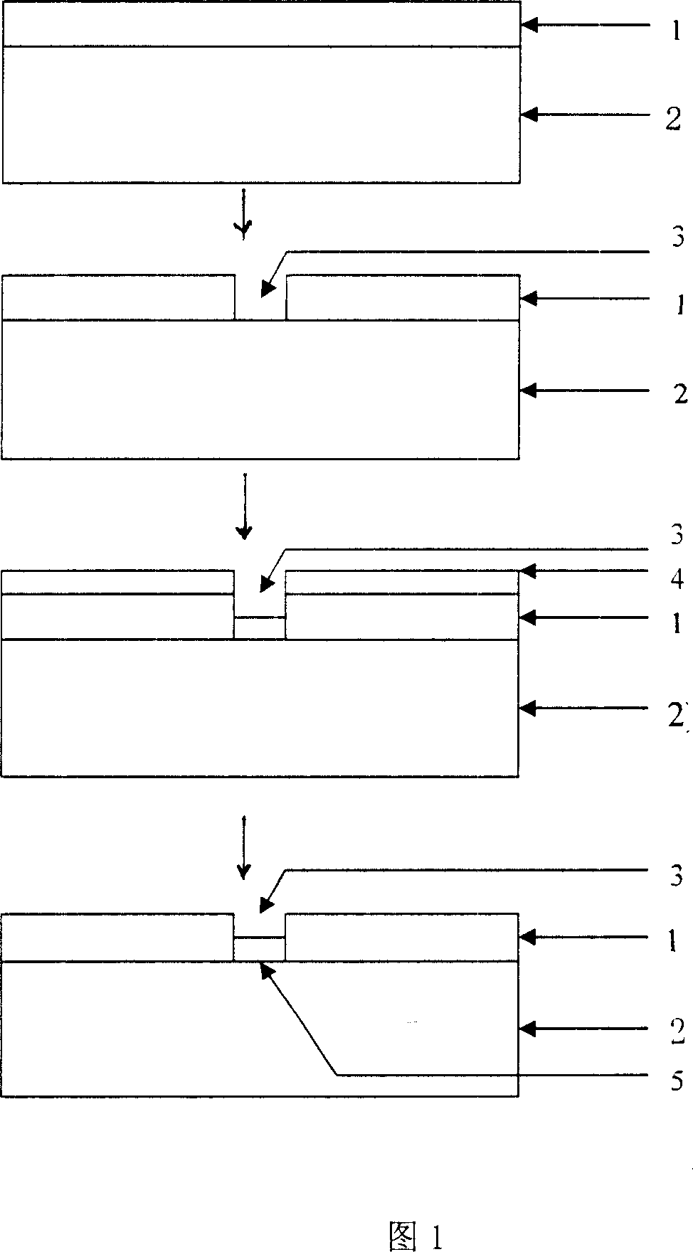
[0037] With reference to Fig. 1, prepare titanium disilicide nanowire of the present embodiment according to the flow process of the present invention:

[0038] 1) On the surface of the monocrystalline silicon substrate 2, a silicon dioxide insulating layer 1 with a thickness of 50 nanometers is grown by a conventional thermal oxidation method, and the thickness of the insulating film 1 is 50 nanometers;

[0039] 2), put the single crystal silicon substrate 2 on which the silicon dioxide insulating layer 1 has been grown in step 1) into the cavity of the focused ion beam system, and use the ion beam to etch the insulating layer with a length of 10 microns and a width of The trench 3 is 14 nanometers; the etching conditions adopted are: ion source voltage 30KV, ion beam current 1pA, beam scanning with beam spot overlapping 50%, and beam dwell time of 1 microsecond; When the groove 3 is etched on the top, and at the same time, a bias voltage is applied on the single crystal sili...

Embodiment 2

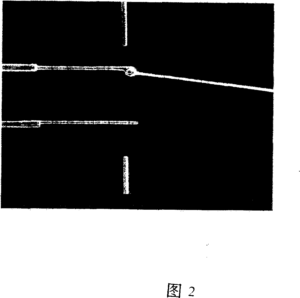
[0044] The specific structure of titanium disilicide nanowires prepared in this embodiment is shown in Figure 2; the nanowires have a line width of 100 nanometers and a length of 30 microns.

[0045] With reference to Fig. 1, the preparation method of the present embodiment is carried out according to the technological process of Fig. 1, and concrete technology is as follows:

[0046] 1. On the surface of the single crystal silicon substrate 2, a 100 nanometer thick aluminum nitride insulating layer 1 is grown by magnetron sputtering, and the thickness of the insulating film i is 100 nanometers;

[0047] 2. Put the silicon substrate 2 already with the aluminum nitride insulating layer 1 into the cavity of the focused ion beam system, and use the ion beam to etch the insulating layer with a length of 30 microns, a width of 100 nanometers, and a depth of 100 nanometer trench 3; the etching conditions adopted are: ion source voltage 30KV, ion beam current 20pA, beam spot overlapp...

Embodiment 3

[0052] The specific structure of titanium disilicide nanowires prepared in this embodiment is shown in Figure 2; the nanowires have a line width of 50 nanometers and a length of 10 microns.

[0053] With reference to Fig. 1, the preparation method of the present embodiment is carried out according to the technological process of Fig. 1, and concrete technology is as follows:

[0054] 1. On the surface of the single crystal silicon substrate 2, a polyimide insulating layer 1 with a thickness of 50 nanometers is coated by a spin coating process, and the thickness of the insulating film 1 is 50 nanometers;

[0055] 2. Put the silicon substrate 2 already covered with the polyimide insulating layer 1 into a conventional electron beam lithography and reactive ion etching system to fabricate nano-grooves. Using traditional electron beam exposure technology, a nanowire pattern with a width of 50 nanometers and a length of 10 nanometers is fabricated on P polyimide. The bias voltage o...


PUM

PropertyMeasurementUnit
widthaaaaaaaaaa
lengthaaaaaaaaaa
thicknessaaaaaaaaaa

Abstract

The method for preparing metal silicides Nano wire with width being as 7 nm includes following steps: developing a layer of insulation film on substrate of monocrystalline silicon; etching grooves in use for producing metal silicides Nano wires through process technology in Nano scale; using method of metal sputtering and coating by vaporization to deposit layer of metal film on silicon substrate with Nano grooves being prepared; carrying out high temperature annealing to make reaction between metal and monocrystalline silicon exposed on bases of grooves so as to produce metal silicides; using chemical corrosion to eat off unreacted metal on surface; producing discrete metal silicides Nano wires in Nano grooves. The method can control position, shape, and width of wire of metal silicides Nano wire to be made. Thus, the invention is applicable to IC to prepare interconnection wires, source pole, drain pole and grid pole based on need.

Description

technical field [0001] The present invention relates to a metal nanowire material and a manufacturing method thereof, in particular not only having a line width of less than 100 nanometers (minimum up to 7 nanometers), but also having a controllable shape and position, used in integrated circuits, microelectronic devices and nanoelectronics The metal silicide nanowire and its manufacturing method have great application prospects in the field of devices and the like. Background technique [0002] Due to the characteristics of low resistivity, high thermal stability and thermal expansion coefficient close to silicon, metal silicide has important applications in micro-nano electronic devices and integrated circuits, such as interconnection wires, source-drain and gate electrodes, etc., especially with As the size of devices decreases, the fabrication of nanoscale metal silicides becomes more and more important. There are roughly two existing technologies for producing metal si...

Claims


Application Information

Patent Timeline
Patent Type & Authority Applications(China)
IPC IPC(8): H01L23/48H01L23/52H01L21/28H01L21/768
CPCH01L2924/0002
Inventor 顾长志岳双林罗强金爱子
Owner INST OF PHYSICS - CHINESE ACAD OF SCI
Why Eureka
Try Eureka