
Method for producing semiconductor chips

a technology of semiconductor chips and semiconductor chips, applied in the direction of manufacturing tools, solid-state devices, laser beam welding apparatus, etc., can solve the problems of small yield, damage to the circuit pattern of the chip, and the appearance of the semiconductor chip is affected, so as to reduce the cost of the chip, suppress the occurrence of defective chips, and shorten the whole treatment process

Active Publication Date: 2021-02-09
FURUKAWA ELECTRIC CO LTD
View PDF16 Cites 1 Cited by
  • Summary
  • Abstract
  • Description
  • Claims
  • Application Information

AI Technical Summary

Benefits of technology

[0012]The present invention was made in view of such problems. Its object is to provide a method for producing semiconductor chips, in which photolithography is not necessary and plasma irradiation can divide (separate) a wafer into chips with more certainty, highly suppressing occurrence of defective chips.
[0017]According to the present invention, plasma irradiation can divide a wafer into chips and thus occurrence of defective chips can be suppressed. At this time, since a mask is formed by using the mask-integrated surface protective tape having the mask material layer on the surface protective tape, photolithography process is not necessary. Thus, equipment for photolithography process is unnecessary, which can reduce the chip cost. Also, a masking process with photoresist is unnecessary and thus the whole treatment process can be shortened.
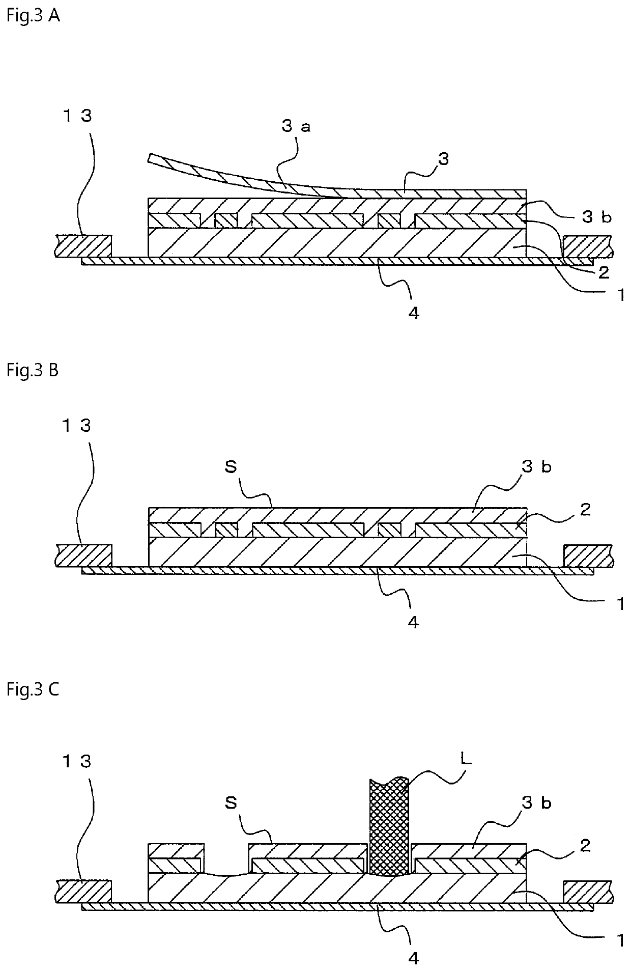
[0018]Also, the mask material layer is removed by using a removing agent and thus, compared with a case in which the mask material layer is removed by ashing for example, damages to a circuit patterned surface of the semiconductor wafer can be prevented.
[0019]Also, using an organic solvent as a removing agent can remove the mask material layer with certainty. In particular, if the removing agent is selected from the group constituting of methyl ethyl ketone, ethanol, ethyl acetate, and any combination thereof, the mask material layer can be removed more efficiently with certainty.
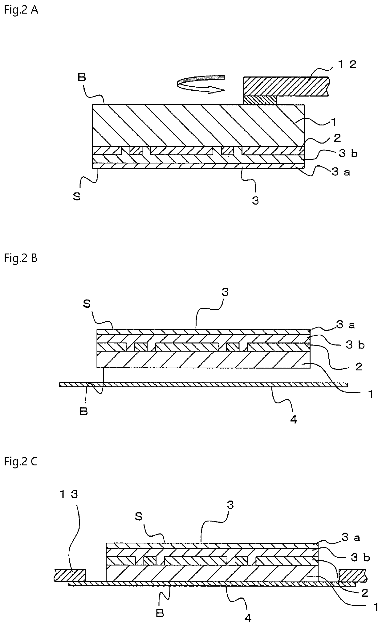
[0020]Also, the removing agent is supplied from above while rotating the separated semiconductor wafer to remove the mask material layer. This can prevent the removing agent from accumulating on the wafer fixing tape, reducing influence of the removing agent to the wafer fixing tape, and, in addition, it is easy to remove the dissolved or peeled mask material layer from the semiconductor wafer.
[0021]The present invention can provide a method for producing semiconductor chips, in which photolithography process is not necessary and plasma irradiation can divide (separate) a wafer into chips with more certainty, highly suppressing occurrence of defective chips.

Problems solved by technology

In particular, IC cards including semiconductor IC chips, such as a memory card and a smart card, require thinning of the chips, and LED / LCD drive devices or the like require downsizing of the chips.
Thus, this cutting resistance may cause the semiconductor chip to have a micro chipping.
The occurrence of the chipping not only impairs appearance of the semiconductor chip but also may invite chip breakage at the time of pickup due to insufficient transverse strength in some cases and may possibly damage circuit patterns on the chip.
As a result, the number of chips that can be obtained from a wafer (an yield) is small.
Furthermore, long processing time of the wafer has also been an issue.
However, there is an inconvenience that the wafer surface may be contaminated with a sublimate from the laser cutting, and thus a pretreatment for protecting the wafer surface using a predetermined liquid protective material may be required in some cases.
Also, although it is called as a dry process, a complete dry process has not been achieved yet.
However, line-by-line processing remains the same, and manufacturing of microchips still requires a certain amount of time.
This method may cause a problem for materials such as a MEMS device or CMOS sensor in which prevention of surface contamination is highly essential.
Also, there is a limit in reducing of the kerf width, and the yield of the obtained chip may be low.
However, the transverse strength of the chip may tend to decrease due to thermal history during formation of the modifying layer, and also there may be silicon debris generated at the time of expansion and separation.
Furthermore, collision between neighboring chips may lead to insufficiency in the transverse strength.
With this technique, the disadvantages of the above processes are improved.
However, since the wafer is separated during the grinding process of the back surface, there may be, in some cases, a phenomenon in which neighboring chip end faces collide with each other, causing chipping off of corners of the chips.
Thus, to perform the plasma dicing, other than equipment for plasma dicing, equipment for photolithography process is also required, which leads to a problem of a rise in the chip cost.
Also, there also has been an inconvenience that the whole treatment process takes a long time because the process needs to go through masking steps with photoresist.

Method used


Image

  • Method for producing semiconductor chips
  • Method for producing semiconductor chips
  • Method for producing semiconductor chips

Examples


first embodiment

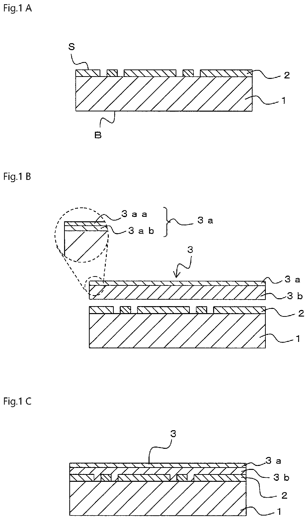
[0050]A first embodiment of the producing method of the present invention will be described with reference to FIG. 1 to FIG. 5. A semiconductor wafer 1 includes a patterned surface 2 on which a semiconductor element circuit or the like is formed on a top surface S thereof (see FIG. 1A). On the side of the patterned surface 2 of the semiconductor wafer 1, a mask-integrated surface-protective tape 3 is pasted (see FIG. 1B). Accordingly, the semiconductor wafer 1 having the patterned surface 2 covered with the mask-integrated surface-protective tape 3 is obtained (see FIG. 1C).

[0051]The mask-integrated surface-protective tape 3 includes a surface protective tape 3a, which is a laminate of a substrate film 3aa and a temporary adhesive layer 3ab, and a mask material layer 3b, which is provided on the temporary adhesive layer 3ab. That is, the mask-integrated surface-protective tape 3 has the surface protective tape 3a and the mask material layer 3b that is provided on the surface protect...

second embodiment

[0101]A second embodiment shown in FIG. 6A to 6C is different from the first embodiment in that the second embodiment includes a step of curing the temporary adhesive layer 3ab by irradiating radioactive rays such as ultraviolet rays onto the mask-integrated surface-protective tape 3 before the step of peeling off the surface protective tape 3a in the above-mentioned first embodiment. The other steps are the same as the first embodiment.

[0102]That is, firstly, the mask-integrated surface-protective tape 3 is pasted onto a side of the top surface S of the semiconductor wafer 1, the wafer fixing tape 4 is pasted onto the grinded back surface B of the semiconductor wafer 1, and the semiconductor wafer 1 is fixed to and supported by the ring frame 13 (see FIG. 2C and FIG. 6A). After that, ultraviolet rays (UV19) are irradiated toward the mask-integrated surface-protective tape 3 from the side of the top surface S (see FIG. 6B). Then, the temporary adhesive layer 3ab of the mask-integrat...

working examples

[0105]Hereinafter, the present invention will be described in further detail based on working examples. However, the present invention is not limited to these examples.

[0106](Surface Protective Tape 3a)

[0107]100 pts.mass of an acrylic polymer B (Mw: 350,000, acid value: 7 mgKOH / g, hydroxyl value: 60 mgKOH / g) including constituent elements with respective molar ratio of 74 mol % of lauryl acrylate, 6 mol % of methyl acrylate, and 20 mol % of 2-hydroxy ethyl acrylate is mixed with 1.0 pts.mass of an isocyanate curing agent (product name: L-45 by Tosoh Corporation) to obtain a temporary adhesive composition A.

[0108]Separately, the substrate film 3aa is formed from low-density polyethylene (LDPE) resin (product name: Nipolon Hard 205 by Tosoh Corporation) and ethylene-acetate vinyl copolymer (EVA) resin (product name: Ultrathene 540 by Tosoh Corporation) by using an extrusion method to have a thickness of 110 μm.

[0109]The above-mentioned temporary adhesive composition A is applied onto ...


PUM

PropertyMeasurementUnit
thicknessaaaaaaaaaa
thicknessaaaaaaaaaa
thicknessaaaaaaaaaa

Abstract

A surface side is irradiated with an SF6 gas plasma to etch a semiconductor wafer which has been peeled off in street portions, and divide the semiconductor wafer into a plurality of individual semiconductor chips. A removing agent is subsequently supplied from the surface side. At that time, it is preferable that the semiconductor wafer divided into the plurality of chips is rotated at high speed. Accordingly, a mask material layer remaining on the surface is removed by the removing agent. Moreover, the removing agent is preferably an organic solvent, and more preferably, methyl ethyl ketone, ethanol, and ethyl acetate, or a combination of these.

Description

TECHNICAL FIELD[0001]The present invention relates to a method for producing a semiconductor chip.BACKGROUND[0002]In recent years, considerable progress has been made in thinning and downsizing of semiconductor chips. In particular, IC cards including semiconductor IC chips, such as a memory card and a smart card, require thinning of the chips, and LED / LCD drive devices or the like require downsizing of the chips. With increase in demands for these products, it is considered that there will be even more needs for thinning and downsizing of semiconductor chips in the future.[0003]These semiconductor chips are obtained by reducing a thickness of a semiconductor wafer to a predetermined thickness through processes such as backgrinding and etching and then divided into individual chips through a dicing process. In such a dicing process, a blade-dicing method in which a dicing blade is used to cut the wafer has been in use. In the blade-dicing method, cutting resistance from the blade is...

Claims


Application Information

Patent Timeline
Patent Type & Authority Patents(United States)
IPC IPC(8): H01L21/311H01L21/308H01L21/683H01L21/78H01L21/3065
CPCH01L21/31133H01L21/3086H01L21/6836H01L21/78H01L21/3065H01L2221/68327H01L2221/68386C09J201/00H01L2221/6834H01L2221/68381H01L21/3081H01L21/02041H01L21/304H01L21/67092H01L21/67132H01L21/68764H01L21/76B23K26/38
Inventor UCHIYAMA, TOMOAKIAKUTSU, AKIRAYOKOI, HIROTOKI
Owner FURUKAWA ELECTRIC CO LTD
Learn More