Low CTE power and ground planes

a ground plane and low cte technology, applied in the field of low cte power and ground planes, can solve the problems of pcbs being associated with pcbs, pcbs being generally more complex, and many systems today cannot tolerate extended down time necessary, and achieve the effect of easy fractur

Inactive Publication Date: 2002-05-02
GLOBALFOUNDRIES INC
View PDF4 Cites 33 Cited by
  • Summary
  • Abstract
  • Description
  • Claims
  • Application Information

AI Technical Summary

Benefits of technology

[0027] Since the copper layer formed by the metallizing process is generally too thin to form a suitable electrical bridge between the two layers of the board, copper electroplating is used to deposit a heavy layer of copper in the holes in order to form a suitable copper cross section for carrying current. Copper plating can be followed by tin-lead or tin plating in order to improve solderability.
[0031] Power core 110 in FIG. 4 comprises a dielectric layer 114 sandwiched between two copper layers 112 and 115. Copper layers 112 and 115 may be thicker than copper layers 102 and 104 to provide extra current carrying capability. Power core 110 is a CCL on which no processing has been performed. Copper layer 112 will become the power plane of a PCB, while copper layer 115 will become the ground plane of a PCB (or vice versa). Power core 111 is a representation of power core 110 after power core 110 has been patterned. Power core 111 comprises copper layers 112 and 115 that are now patterned and dielectric layer 114. Copper layer 112 is patterned with two clearance areas 182 and 179, while copper layer 115 is patterned with two clearance areas 184 and 180. These clearance areas will prevent the power and ground planes from contacting PTHs that will be drilled in these locations after power core 111 has been pressed into a composite and holes have been drilled and plated.
[0033] Several PTHs are shown in PCB 120. PTH 109 connects power plane 112 to a C4 ball 107, a line on patterned copper layer 105, and a line on signal core layer 135. Clearance area 180 prevents PTH 109 from connecting to ground. Note that clearance area 180 would be filled with reflowed dielectric after lamination, but this is not shown in FIG. 4 for simplicity. PTH 108 connects signal lines on copper layers 102, 105, 132, and 135, and the signal line on copper layer 102 also connects to a C4 ball 107. Clearance areas 184 and 182 prevent PTH 108 from contacting ground plane 115 or power plane 112, respectively. PTH 106 connects ground plane 115 with lines or pads on copper layers 135, 132, and 102.
[0035] This can be seen in FIG. 4, where chip 160 is directly connected to metal layer 102 of PCB 120. If the PCB expands with increasing temperature, the expansion caused by a relatively high CTE, C4 balls 107 move with the PCB. The C4 balls 107 are directly connected to the chip, and the chip must absorb the tensile stress caused by the increase in distance between the balls 107. Unfortunately, semiconductor chips are primarily silicon, which is crystalline. The chip itself is easily fractured because of its structure and the balls can also pull away from the chip.

Problems solved by technology

Many systems today cannot tolerate the extended down time necessary to replace failed components that make up the computer system.
PCBs are generally more complex, however, and are usually made of conductive, metal power and ground planes and several signal planes containing circuit lines sandwiched between several layers of insulator, with metal lines and pads on the top and bottom surface of the sandwich.
There are, however, problems associated with PCBs.
One of the causes of some of these problems is the coefficient of thermal expansion (CTE) for the overall PCB and the individual layers.
However, the effectiveness of using these lower CTE dielectrics is limited because the power and ground planes, which constitute a significant portion of the PCB, are still composed of copper.
Sometimes these devices or the electrical connections between them cannot withstand the stress, particularly after repeated temperature cycling.
These stresses are particularly deleterious for LCCs.
Unfortunately, because chips are primarily made of crystalline silicon, which is easily fractured, this stress can either fracture the C4 connections or the chip / LCC CTE mismatch will cause the assembled package to warp putting tensile stress on the chip, possibly cracking the chip.
This difference in expansion can put high stresses on the dielectrics, which can lead to cracking of the dielectric materials.
Cracking of dielectrics can cause opens because lines can be pulled apart.
Shear induced debonding exacerbates the CTE-caused cracking mechanisms because the debonded dielectric is essentially "floating" and is not connected to the metallic power / ground planes.
While low CTE metals such as invar, stainless steel, and molybdenum have been used to construct lower CTE power planes for PCBs and LCCs, use of these alternative metals can create a variety of manufacturing complications.
These complications include galvanic activity and corrosion, multi-step etching, and complicated waste treatment.
Therefore, without a way to limit failures and fractures caused by CTE differences between dielectrics and power / ground layers and the overall relatively high CTE in PCBs and LCCs, PCBs and LCCs will continue to have a higher numbers of failures and reliability problems.

Method used


Image

  • Low CTE power and ground planes
  • Low CTE power and ground planes
  • Low CTE power and ground planes

Examples


Embodiment Construction

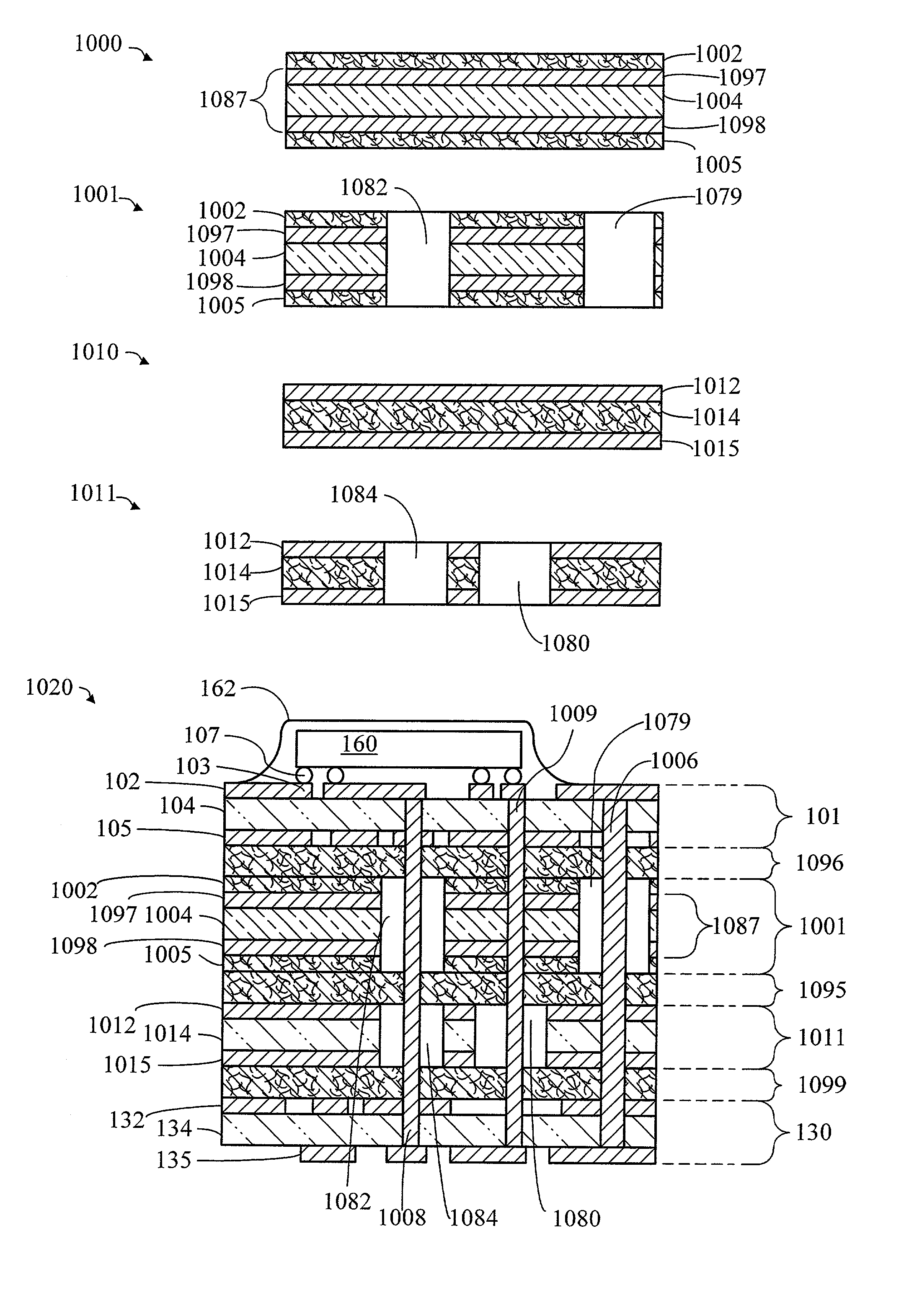
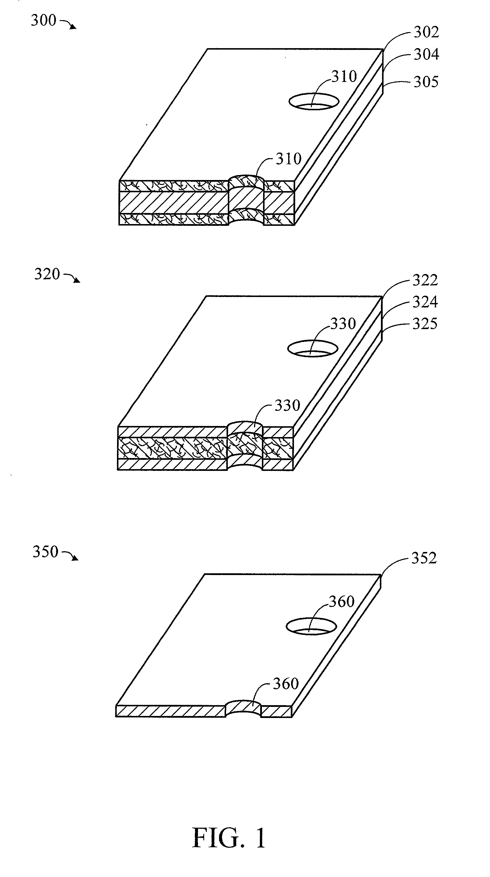
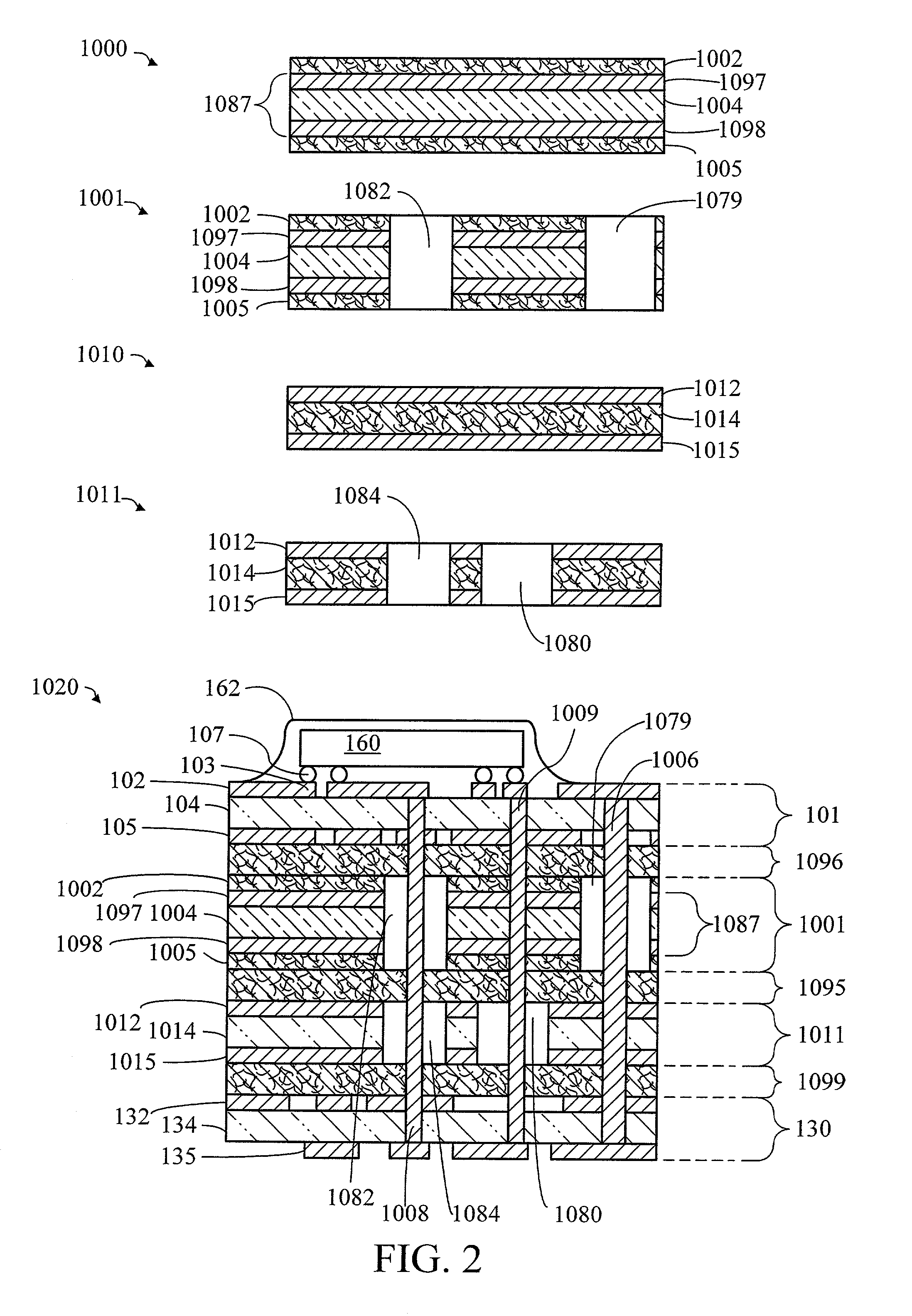
[0036] The preferred embodiments of the present invention overcome the limitations of the prior art by providing conductive materials having low CTEs that are used for power and ground planes in Printed Circuit Boards (PCBs) and PCBs used as Laminate Chip Carriers (LCCs). By providing low CTE materials for power and ground planes in PCBs, the overall CTE of the PCB can be lowered, which decreases the chances of chip failure, dielectric cracking, and shear induced debonding. In addition, the problems (galvanic activity and corrosion, multi-step etching, and complicated waste treatment) associated with the use of the exotic, low CTE metals are completely eliminated or dramatically reduced.

[0037] Before proceeding to the preferred embodiments, a short discussion of terminology is beneficial. As stated in the Overview section, "prepreg" is a term that generally connotes fiberglass and epoxy resin. This is often termed "prepreg" because the fiber is impregnated with resin during processi...


PUM

PropertyMeasurementUnit
thicknessaaaaaaaaaa
thicknessaaaaaaaaaa
coefficient of thermal expansionaaaaaaaaaa

Abstract

Conductive materials that have low coefficients of thermal expansion (CTEs) and that are used for power and ground planes are disclosed. Fibrous materials (such as carbon, graphite, glass, quartz, polyethylene, and liquid crystal polymer fibers) with low CTEs are metallized to provide a resultant conductive material with a low CTE. Such fibers may be metallized in their individual state and then formed into a fabric, or these materials may be formed into a fabric and then metallized or a combination of both metallizations may be used. In addition, a graphite or carbon sheet may be metallized on one or both sides to provide a material that has a low CTE and high conductivity. These metallized, low CTE power and ground planes may be laminated with other planes / cores into a composite, or laminated into a core which is then laminated with other planes / cores into a composite. The resultant composite may be used for printed circuit boards (PCBs) or PCBs used as laminate chip carriers.

Description

[0001] This application is related to a copending patent application by Japp et al., entitled "POROUS POWER AND GROUND PLANES FOR REDUCED PCB DELAMINATION AND BETTER RELIABILITY", serial number______, filed______, and is incorporated herein by reference.[0002] 1. Technical Field[0003] The present invention relates generally to the field of computer manufacturing and more specifically to reducing the coefficient of thermal expansion of boards used in computers.[0004] 2. Background Art[0005] Computers and similar electronic equipment have become ubiquitous elements in the lives of people. Many businesses, banks, and governments rely on computers for their everyday activities. A large portion of the global community require that computers be reliable, stable facets of their economic, societal, and communication foundations. Computers today are required to run longer, with less down-time, than at any time in the past.[0006] Because computers are so necessary, there has been an increased...

Claims


Application Information

Patent Timeline
Patent Type & Authority Applications(United States)
IPC IPC(8): H05K1/03H05K3/46
CPCH05K1/0366H05K3/4641H05K2201/0141H05K2201/0158H05K2201/0278H05K2201/0281Y10T29/49165H05K2201/0323H05K2201/068H05K2201/09309Y10S428/901Y10T29/49126H05K2201/029
Inventor JAPP, ROBERT M.POLIKS, MARK D.
Owner GLOBALFOUNDRIES INC
Why Eureka
Try Eureka