Semiconductor thin film forming method, production methods for semiconductor device and electrooptical device, devices used for these methods, and semiconductor device and electrooptical device

a technology of semiconductor devices and thin films, applied in the direction of polycrystalline material growth, crystal growth process, chemically reactive gases, etc., can solve the problems of increasing the cost of apparatus, poor productivity, and difficulty in obtaining crystals with a grain size of 500 nm or mor

Inactive Publication Date: 2003-01-16
SONY CORP
View PDF18 Cites 349 Cited by
  • Summary
  • Abstract
  • Description
  • Claims
  • Application Information

AI Technical Summary

Benefits of technology

[0011] In forming a polycrystalline or a single crystalline semiconductor thin-film on a substrate, or in forming a semiconductor device having a polycrystalline or a single crystalline semiconductor thin-film on a substrate, a method for forming a semiconductor thin-film or for manufacturing a semiconductor device, according to the present invention, comprises a first step of forming a low-crystallization semiconductor thin-film on the substrate, and a second step of heating and cooling the low-crystallization semiconductor thin-film to a fusion, a semi-fusion, or a non-fusion state by flash lamp annealing to facilitate the crystallization of the low-crystallization semiconductor thin-film.
[0012] In addition, as an apparatus for performing the method of the present invention, the present invention provides a forming apparatus for forming a polycrystalline or a single crystalline semiconductor thin-film or a manufacturing apparatus for manufacturing a semiconductor device, in which the apparatus comprises first means for forming a low-crystallization semiconductor thin-film on the substrate, and second means for heating and cooling the low-crystallization semiconductor thin-film to a fusion, a semi-fusion, or a non-fusion state by flash lamp annealing to facilitate the crystallization of the low-crystallization semiconductor thin-film.

Problems solved by technology

As a result, even when a method is performed in which substrate temperature is heated to approximately 400.degree. C. while short wavelength and short pulse laser is emitted, and in which hydrogen, oxygen, and the like which inhibit the crystal growth are sufficiently removed so as to control the solidification speed, it has been difficult to obtain crystals having a grain size of 500 nm or more.
However, there have been a number of problems, such as unstable excimer laser output, poor productivity, increase in cost of apparatus due to increased size thereof, lower yield, degradation in quality, and the like, and in particular, when a large glass substrate having a size of 1 meter by 1 meter is used, the problems mentioned above become more serious, and as a result, it becomes more difficult to improve performance and quality and to reduce cost.
However, the process is complicated, sufficient gettering effect cannot be obtained, semiconductor properties of the silicon film are degraded, and the stability and the reliability of elements thus formed are degraded.
Hence, it is difficult to reduce cost, and the applications are limited to EVF and data / AV projectors.
In a catalytic CVD method, without performing anneal for crystallization, a carrier mobility of approximately 30 cm.sup.2 / V.multidot.sec has been obtained; however, the value mentioned above is not large enough to manufacture superior MOSTFTs.
In addition, when a polycrystalline silicon film is formed on a glass substrate, amorphous silicon in an initial transition state (a thickness of 5 to 10 nm) may be easily formed depending on film-forming conditions, and when a bottom-gate MOSTFT is formed, it is difficult to obtain desired carrier mobility.
In general, in an LCD which uses polycrystalline silicon MOSTFTs and which is integrated with driving circuits, bottom-gate MOSTFTs are preferably formed in view of yield and productivity; however, the problem described above has been still serious.

Method used


Image

  • Semiconductor thin film forming method, production methods for semiconductor device and electrooptical device, devices used for these methods, and semiconductor device and electrooptical device
  • Semiconductor thin film forming method, production methods for semiconductor device and electrooptical device, devices used for these methods, and semiconductor device and electrooptical device
  • Semiconductor thin film forming method, production methods for semiconductor device and electrooptical device, devices used for these methods, and semiconductor device and electrooptical device

Examples


fourth embodiment

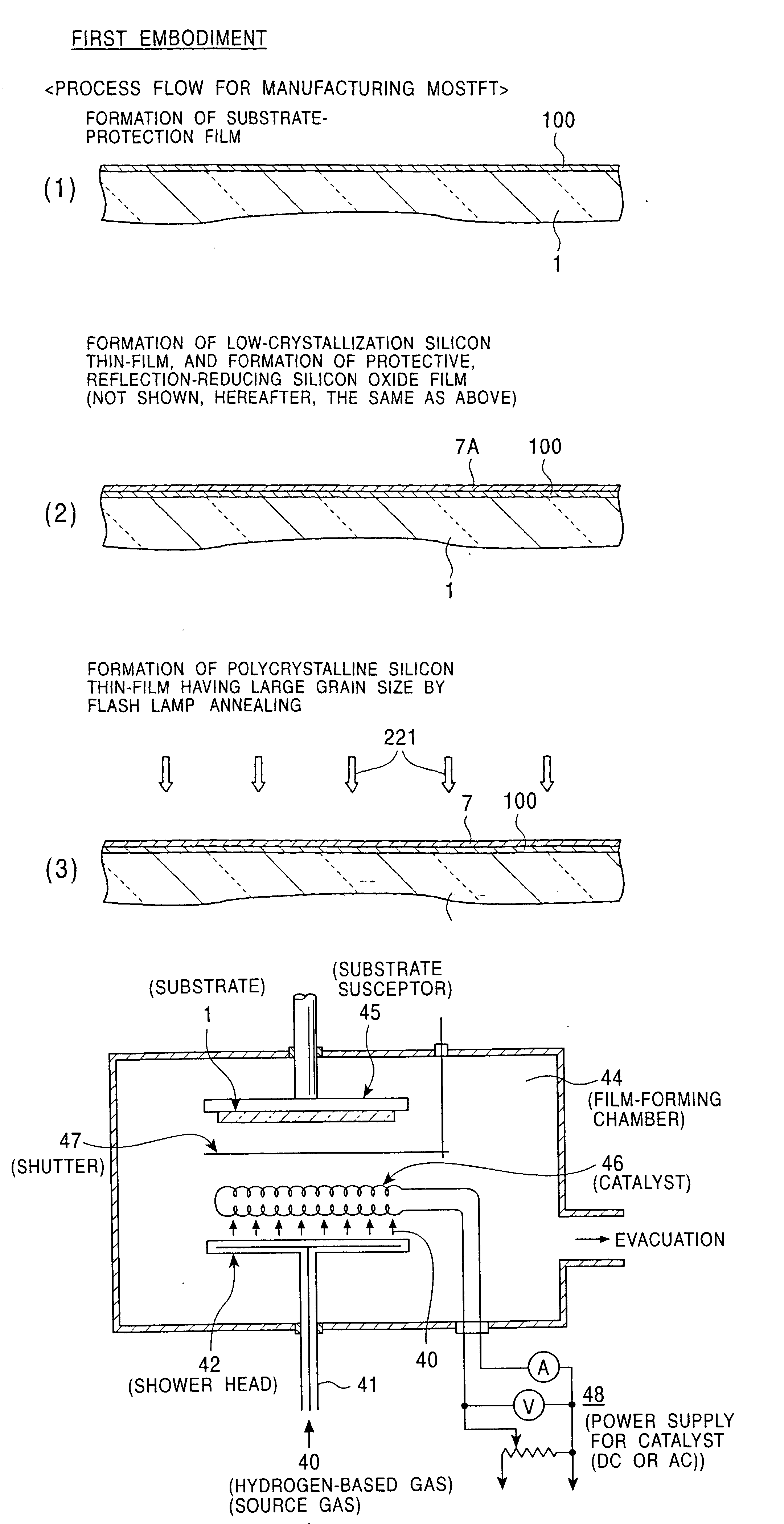
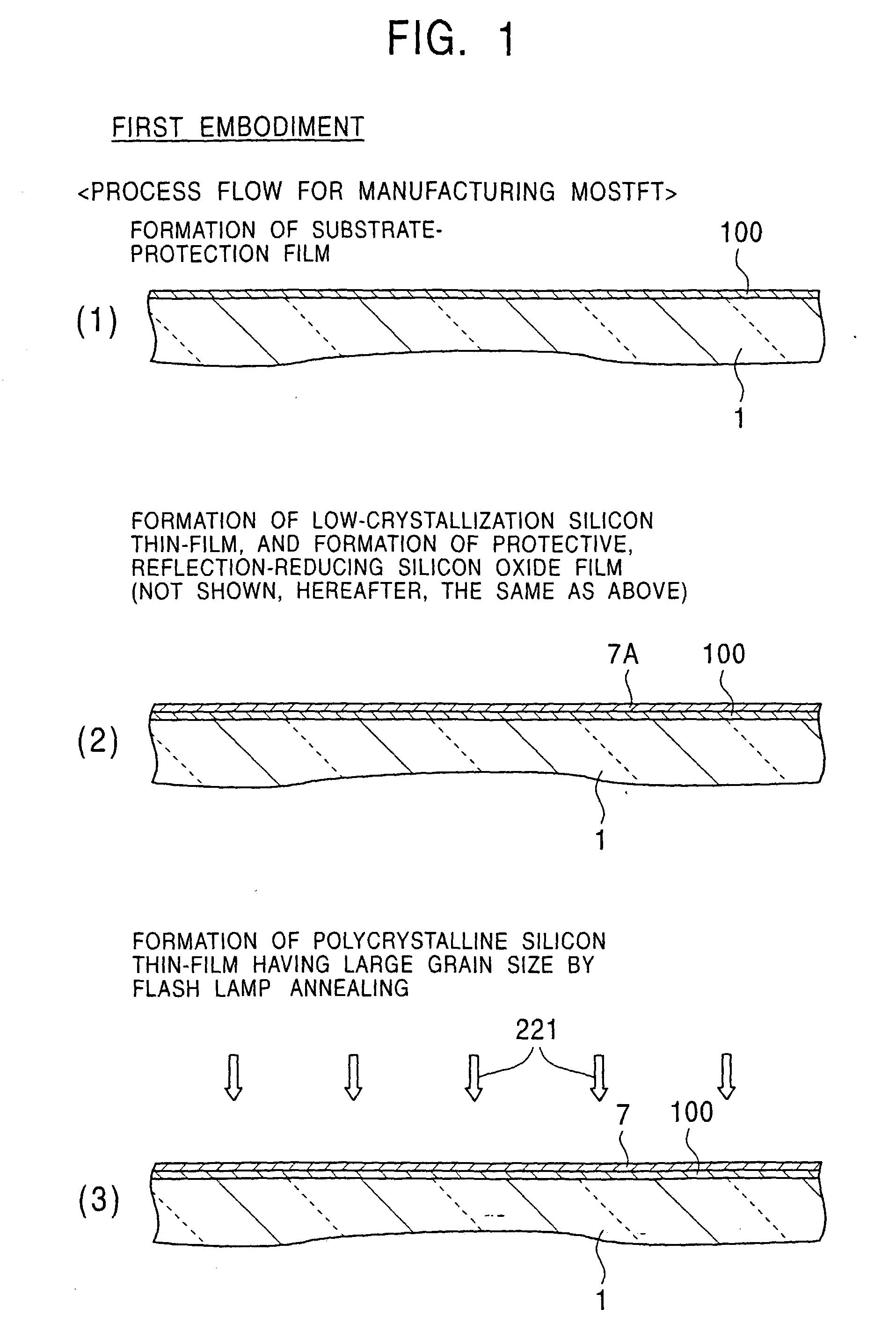
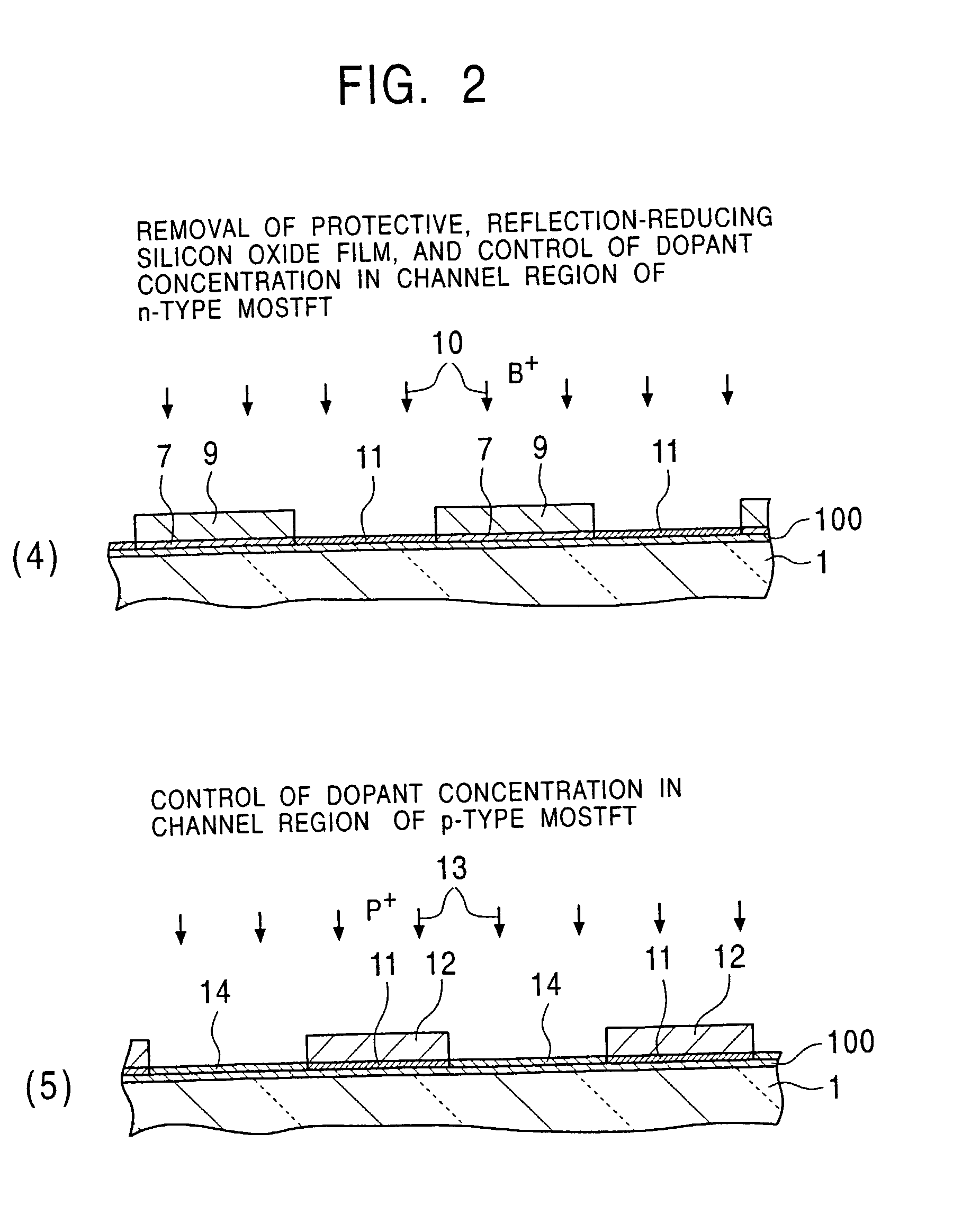
[0607] Fourth Embodiment

[0608] In this embodiment, the present invention is applied to a field emission type (FED) display devices. Hereinafter, the structural examples and the manufacturing examples thereof will be described. In this embodiment, a top gate type MOSTFT will be described, and it is naturally understood that the present invention be applied to a bottom gate type or a dual gate type MOSTFT.

[0609]

[0610] As shown in FIGS. 50(A), (B), and (C), according to this structural example I, by using the polycrystalline silicon thin-film, which may or may not contain tin and which has a large grain size and high crystallinity, formed by the method described above according to the present invention on the substrate 111 composed of glass or the like, the gate channel regions 117, the source regions 120, and the drain regions 121 of the switching MOSTFT 1 and the current driving MOSTFT 2 are formed. In addition, the gate electrodes 115 are formed on the gate insulating film 118, and...

fifth embodiment

[0656] Fifth Embodiment

[0657] In this embodiment, the present invention is applied to a solar cell which is a photoelectric transfer device. A manufacturing example thereof will be described below.

[0658] First, as shown in FIG. 56(1), the n-type low-crystallization silicon film 7A (100 to 200 nm thick) is formed by plasma CVD, catalytic CVD, or the like on the metal substrate 111 formed of stainless steel or the like. In this case, an n-type dopant such as PH.sub.3 is appropriately contained in monosilane so as to have a concentration of 1.times.10.sup.19 to 1.times.10.sup.20 atoms / cc. In addition, when necessary, a thin-film (100 to 300 nm thick) of a high melting point metal (Ti, Ta, Mo, W, or an alloy thereof, such as a Mo--Ta alloy) or a metal silicide (WSi.sub.2, MoSi.sub.2, TiSi.sub.2, TaSi.sub.2, or the like) is formed on the metal substrate or a glass substrate by sputtering, CVD, or the like.

[0659] Continuously, by plasma CVD, catalytic CVD, or the like, an i-type low-cryst...


PUM

PropertyMeasurementUnit
emission timeaaaaaaaaaa
pressureaaaaaaaaaa

Abstract

An object of the present invention is to provide a method for easily forming a polycrystalline semiconductor thin-film, such as polycrystalline silicon having high crystallinity and high quality, or a single crystalline semiconductor thin-film at inexpensive cost, the crystalline semiconductor thin-film having a large area, and to provide an apparatus for processing the method described above. In forming a polycrystalline (or single crystalline) semiconductor thin-film (7), such as a polycrystalline silicon thin-film, having high crystallinity and a large grain size on a substrate (1), or in forming a semiconductor device having the polycrystalline (or single crystalline) semiconductor thin-film (7) on the substrate (1), a method comprises forming a low-crystallization semiconductor thin-film (7A) on the substrate (1), and subsequently heating and cooling this low-crystallization semiconductor thin-film (7A) to a fusion, a semi-fusion, or a non-fusion state by flash lamp annealing to facilitate the crystallization of the low-crystallization semiconductor thin-film, whereby a polycrystalline (single crystalline) semiconductor thin-film (7) is obtained. A method for forming the semiconductor device and an apparatus for processing the methods are also disclosed.

Description

[0001] The present invention relates to methods and apparatuses for growing polycrystalline or a single crystalline semiconductor thin-film, such as polycrystalline silicon, single crystalline silicon, or the like, on a substrate, to methods and apparatuses for manufacturing semiconductor devices and electrooptic devices having the polycrystalline or the single crystalline semiconductor thin-film on the substrate, and to the semiconductor devices and the electrooptic devices.[0002] Heretofore, when a source, a drain, and a channel region of a MOSFET (Metal-Oxide-Semiconductor Field Effect Transistor),such as a MOSTFT (Thin Film Transistor=thin-film insulating gate type field effect transistor) are formed, vapor-phase growth, such as plasma CVD (CVD: Chemical Vapor Deposition), reduced-pressure CVD, or catalytic CVD, solid-phase growth, liquid-phase growth, excimer laser anneal, and the like have been used.[0003] As disclosed in Japanese Unexamined Patent Application Publication Nos....

Claims


Application Information

Patent Timeline
Patent Type & Authority Applications(United States)
IPC IPC(8): C23C16/24C23C16/56C30B13/24H01L21/20H01L21/336H01L29/786
CPCC23C16/24C23C16/56C30B13/24H01L21/2022H01L27/3211H01L27/3248H01L27/3272H01L29/66757H01L29/66765H01L29/6678H01L29/78648H01L29/78675H01L29/78678H01L29/78681H01L29/78684H01L51/5284H01L2251/5315H01L21/02576H01L21/02488H01L21/02422H01L21/02502H01L21/02535H01L21/02529H01L21/0242H01L21/02527H01L21/0262H01L21/02425H01L21/02598H01L21/02532H01L21/02579H01L21/02595H01L21/02546H01L21/02381H01L21/02691H10K59/35H10K59/123H10K59/126H10K50/865H10K2102/3026H01L21/20B82Y40/00H01L21/02672
Inventor YAMANAKA, HIDEO
Owner SONY CORP
Why Eureka
Try Eureka