

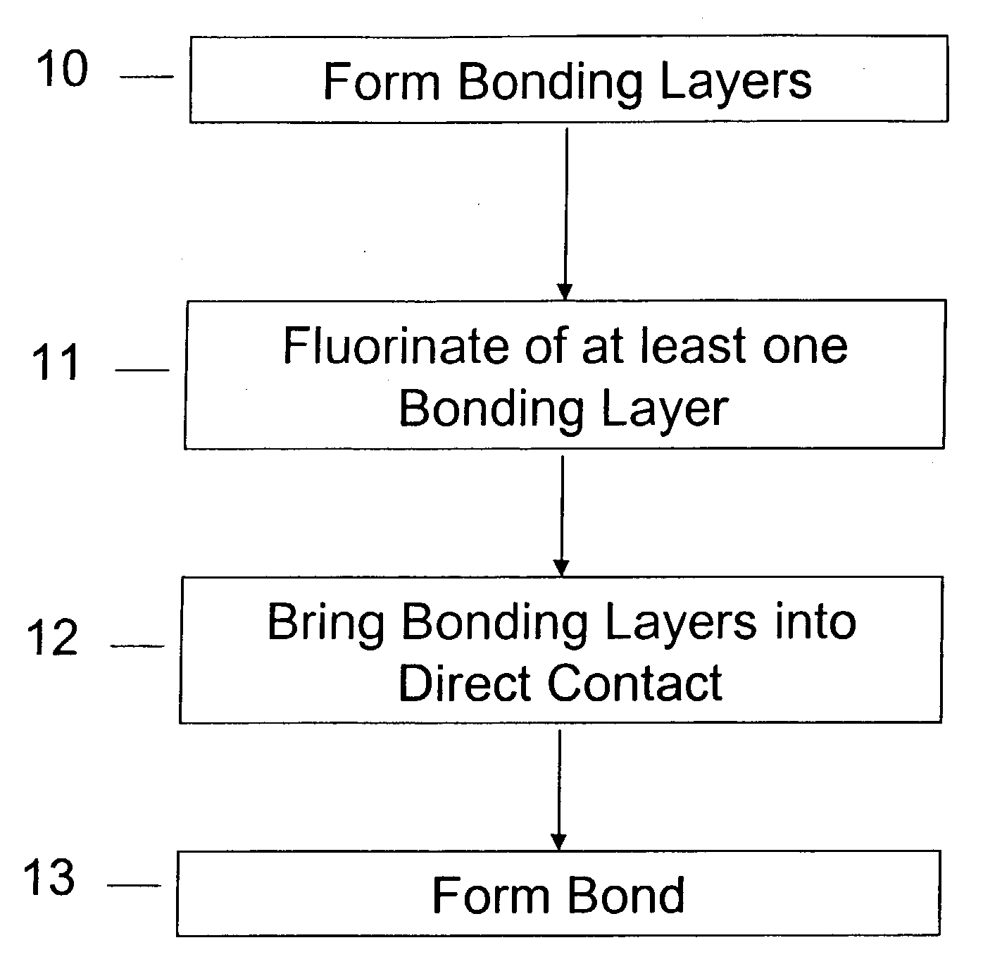
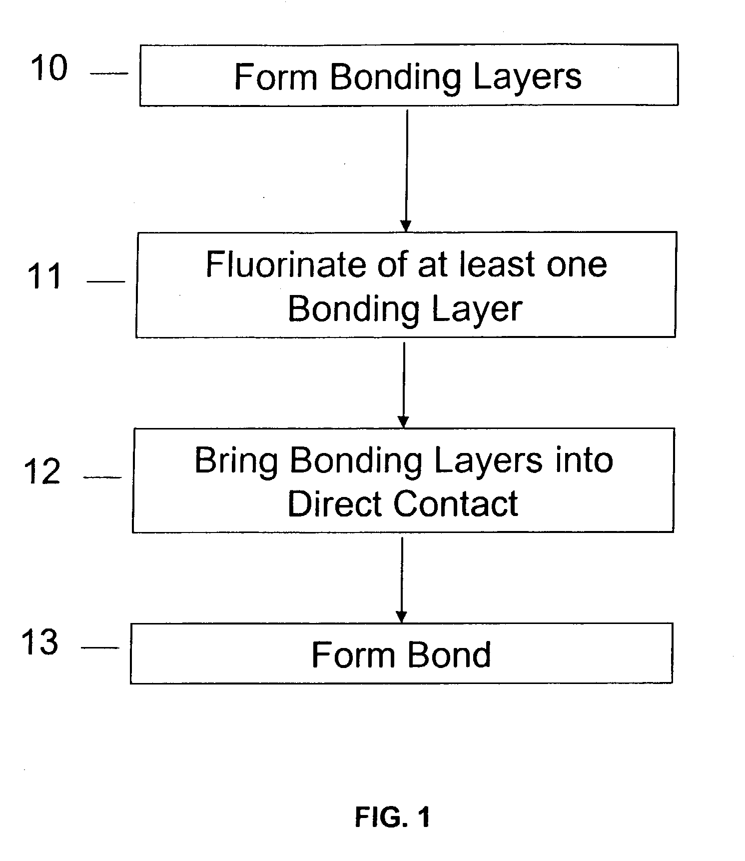
Method of room temperature covalent bonding
- Summary
- Abstract
- Description
- Claims
- Application Information
AI Technical Summary
Benefits of technology
Problems solved by technology
Method used
Image

Examples
first embodiment
[0043] In a first example of the first embodiment, PECVD (Plasma Enhanced Chemical Vapor Deposition) silicon dioxide was deposited on single-side polished silicon wafers at 200-250.degree. C. The thickness of the PECVD oxide is not critical and was arbitrarily chosen as .about.1.0 .mu.m. The wafers covered with the PECVD oxide layers were polished to smooth the surfaces. AFM (Atomic Force Microscopy) was employed to determine the RMS (Root Mean Square) value of surface micro-roughness to be 1-3 .ANG.. The wafers were cleaned by a modified RCA 1 (H.sub.2O:H.sub.2O.sub.2:NH.sub.4-OH=5:1:0.25) solution and spin-dried.
[0044] The wafers were divided arbitrarily into several groups with each wafer pair in a group treated in a specific way prior to bonding. In Group I, the oxide covered wafer pairs were treated in an oxygen plasma for thirty seconds in an reactive ion etch mode (RIE) at 100 mTorr. The plasma treated wafers were dipped in CMOS grade ammonium hydroxide aqueous solution conta...
example
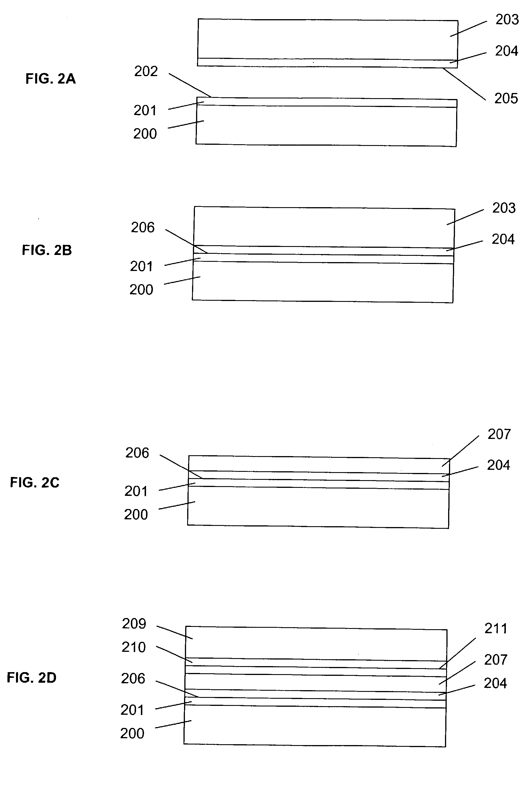
[0075] A second example of the method will be described again using FIGS. 8A-8C. A first oxide layer 81 is formed on substrate 80 (FIG. 8A). Fluorine is introduced into film 81 by one of the procedures described above, namely, exposure to HF or exposure to a F-containing gas. A second oxide film 82 is formed on film 81 by PECVD, for example (FIG. 8B). Fluorine is introduced into the second film by diffusion and / or surface segregation. It may also be introduced into the second film by the use of an appropriate F-containing precursor for the deposition of said oxide film 82. It is noted that the dimensions of films 81 and 82 are not to scale for this example, since the figures were also used to describe an example where film 82 is formed in the surface of film 81, but the figures do accurately represent the position of films 81 and 82. In this example, the structure does not need to be baked to create a fluorinated layer that assists in the removal of reaction byproducts because of th...
PUM
| Property | Measurement | Unit |
|---|---|---|
| Fraction | aaaaa | aaaaa |
| Force | aaaaa | aaaaa |
| Force | aaaaa | aaaaa |
Abstract
Description
Claims
Application Information