Intergrated photonic crystal structure and method of producing same

Inactive Publication Date: 2004-12-30
IGNIS PHOTONYX
View PDF12 Cites 74 Cited by
  • Summary
  • Abstract
  • Description
  • Claims
  • Application Information

AI Technical Summary

Benefits of technology

0085] An advantage of the method according to the invention is that a waveguide or component will be formed in a single etching process after the end of the growth process and this hereby simplifies the fabrication of a three dimensional photonic crystal waveguide or component. However, the formation of a structure in accordance with one preferred embodiment of the present invention, two etching processes will be required at the end of the growth process, to form the two sets of essentially straight passages in two distinct directions through the layered structure.
0086] Another advantage is that the method eliminates the need for complex alignment and multiple intermediate processing steps between features of the individual layers.
0087] Another advantage of the method of the present invention is that it avoids lengthy and handling-critical processes such as polishing or thinning after the application of each layer. Another advantage is that the method consists of steps that are conventio

Problems solved by technology

These types of photonic crystals, if designed for infrared or optical light, are difficult to fabricate, since the spatial periods must be comparable to the wavelength of operation.
However, the introduction of wanted defects into three-dimensional photonic crystals without introducing unwanted defects during processing is difficult.
These unwanted defects give rise to serious energy losses for the resonant cavity or waveguide structures.
However, the greatest problem and technological challenge in connection with the manufacture of photonic crystals concern the formation of a true three-dimensional structure in an industrial process scale.
However, the use of total internal reflection will only enable partial polarisation dependent band gaps, i.e. band gaps for certain discrete directions of propagation for narrow frequency ranges and only for one of the main polarisation states.
This will lead to substantial radiation loss in waveguides,

Method used


Image

  • Intergrated photonic crystal structure and method of producing same
  • Intergrated photonic crystal structure and method of producing same
  • Intergrated photonic crystal structure and method of producing same

Examples


Example

EXAMPLE 1

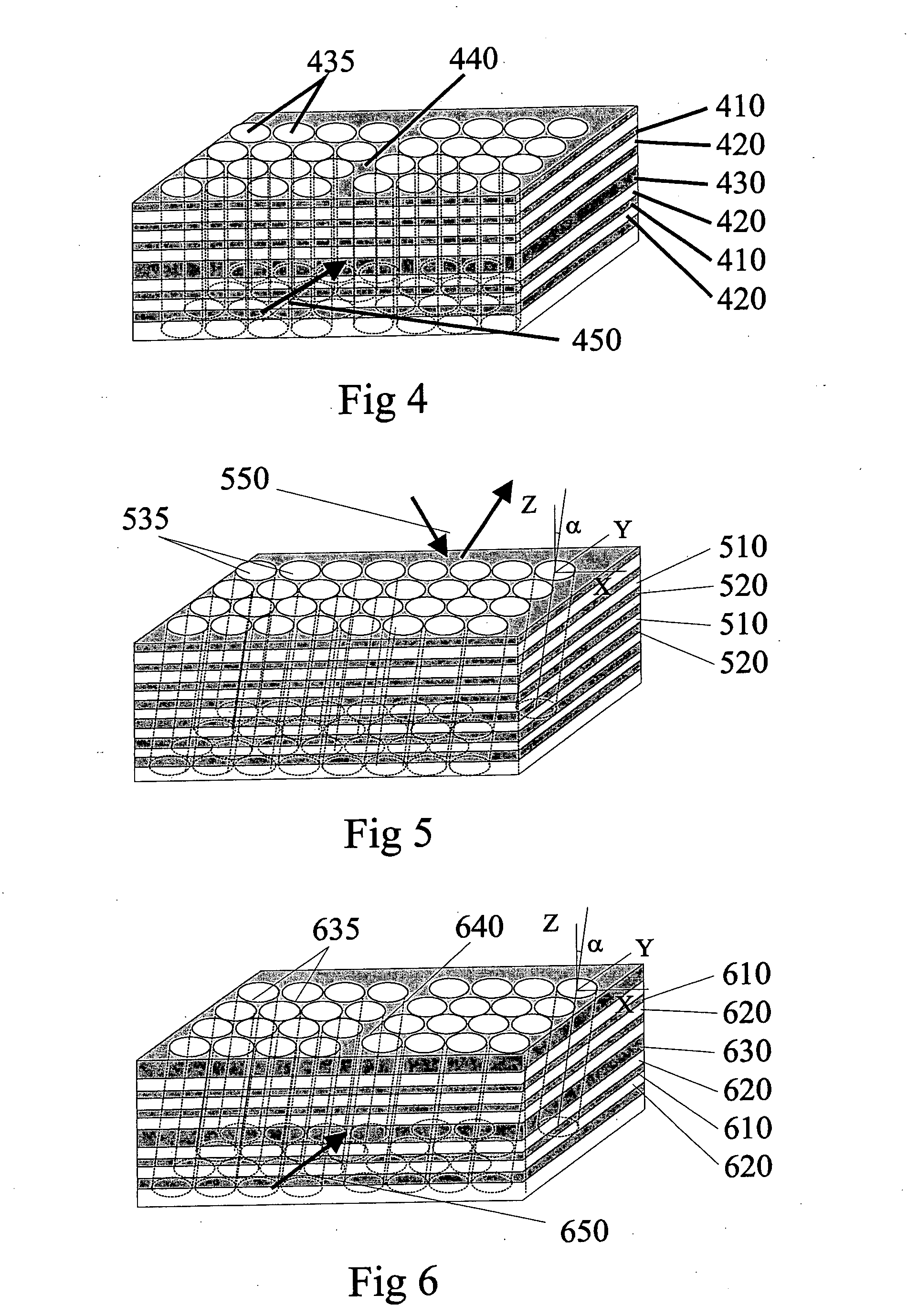
[0155] This example concerns an aspect of the present invention with .alpha.=1.degree.. Said first surface is periodic and two-dimensional with the tangent plane (of said first surface) being a plane parallel to the (x, y) plane of a Cartesian coordinate system (x, y, z). Let a.sub.1=.LAMBDA..sub..zeta.({square root}{square root over (3)} x+y) / 2 and a.sub.2=.LAMBDA..sub..zeta.({square root}{square root over (3)} x-y) / 2 be two basis vectors that span the (x,y) plane characterising a two-dimensional triangular crystal lattice with lattice constant .LAMBDA..sub..zeta., and a.sub.3=.LAMBDA..sub.zz be a third basis vector, x, y, and z being the Cartesian vectors of unit length.

[0156] Said first surface is defined as the set of points (x, y, z=S(.zeta..sub.1, .zeta..sub.2)) where S(.zeta..sub.1, .zeta..sub.2)=A.sub..zeta. sin(2.pi. .zeta..sub.1 / .LAMBDA..sub..zeta.) sin(2.pi. .zeta..sub.2 / .LAMBDA..sub..zeta.)-t.sub.a / 2, where the coordinate pair (.zeta..sub.1,.zeta..sub.2) describ...

Example

EXAMPLE 2

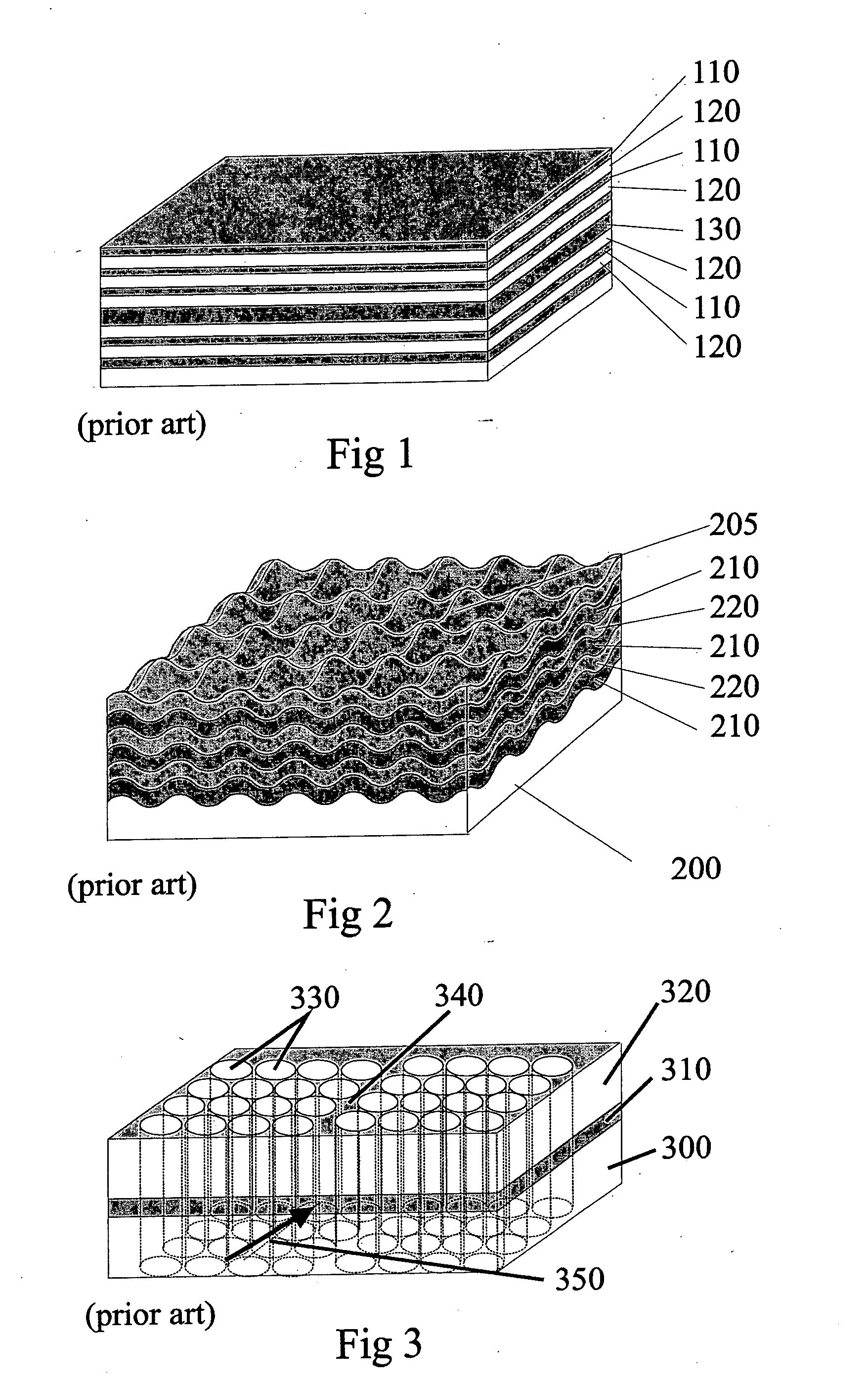
[0160] This example concerns an aspect of the present invention in the case where said first surface is planar and the intersecting angle of the second structure .alpha.=35.26.degree.. In the following the (x,y) plane of a Cartesian coordinate system (x, y, z) is set parallel to the surface. A layered structure is formed by depositing layer A with refractive index n.sub.a and thickness t.sub.a followed by layer B with refractive index n.sub.b and thickness t.sub.b in alternance. The period of this multilayer stack is .LAMBDA..sub.z=t.sub.a+t.sub.b, which is the length of the unit of two layers that is repeated. In this example, the units are repeated an infinite number of times, but in reality approximately 10 to 20 units will be sufficient.

[0161] Let (x', y', z') be a second Cartesian coordinate system where the z'-axis and the z-axis intersect at the angle .alpha., and let a.sub.1=.LAMBDA.({square root}{square root over (3)} x+y) / 2 and a.sub.2=.LAMBDA.({square root}{squar...

Example

EXAMPLE 3

[0165] This example concerns an aspect of the present invention in the case where the first surface is planar and the intersecting angle of the second structure .alpha.=0.degree.. In the following the (x,y) plane of a Cartesian coordinate system (x, y, z) is set parallel to the surface. A layered structure is formed by depositing layer A with refractive index n.sub.a and thickness t.sub.a followed by layer B with refractive index n.sub.b and thickness t.sub.b in alternance. The period of this multilayer stack is .LAMBDA..sub.z=t.sub.a+t.sub.b, which is the length of the unit of two layers that is repeated. In this example, the units are repeated an infinite number of times, but in reality approximately 10 to 20 units will be sufficient.

[0166] Let (x', y', z') be a second Cartesian coordinate system where the z'-axis and the z-axis intersect at an angle .alpha., and let a.sub.1=.LAMBDA.({square root}{square root over (3)} x+y) / 2 and a.sub.2=.LAMBDA.({square root}{square root...


PUM


Abstract

An integrated photonic crystal (IPC) structure and method of producing same is disclosed. The (IPC) structure includes a first layered sub-structure (610, 620) with a surface and a one-dimensional periodic refractive index variation along the direction perpendicular to the surface. This first layered sub-structure enables a photonic band gap or high omnidirectional reflectivity for propagation of radiation having a spectrum of electromagnetic modes incident from a direction perpendicular to the plane of the surface. The PC-structure further includes a first defect (630) in the first layered sub-structure that enables an electromagnetic mode to be localised in the vicinity of the first defect. The electromagnetic radiation is hereby vertically confined. Furthermore, the IPC-structure consists of a second sub-structure with a plurality of essentially straight identical passages (635) arranged in a two-dimensional periodic pattern cutting through the layered structure at an angle alpha. This second sub-structure enables a two-dimensional photonic band gap for propagation of radiation having a spectrum of electromagnetic modes incident from any direction in the plane of the surface. A second defect (640) in the second sub-structure enables an electromagnetic mode to be localised in the vicinity of the second defect. By means of the first and second defects in the first layered and second sub-structures a photonic crystal waveguide may e.g. be constructed (650). This photonic crystal waveguide can control and filter light very efficiently and radiation losses can be minimised significantly. The method is particularly well-suited for providing layered structures in which the layers are non-mono-crystalline. The method is based on standard processing steps and tools from the semiconductor and integrated optics industry such as vapour deposition or sputtering, (photo)lithography and etching. With the invention a basic building block for a high-density integrated optics platform for telecommunications and advanced optical signal processing in general is disclosed.

Description

[0001] The invention relates to the field of photonic crystals. In particular, this invention relates to a photonic crystal structure for the transmission / reflection and filtering of electromagnetic waves. Further the invention relates to a photonic crystal structure wherein waveguide cores and / or reflectors are formed.[0002] The invention also concerns a method for the manufacture of integrated photonic crystal structures for the transmission / reflection and filtering of electromagnetic waves.DESCRIPTION OF RELATED ART[0003] In recent years periodic dielectric media, so called photonic crystals, have drawn a lot of interest in the research community, and many structures have been studied theoretically and experimentally. Photonic crystals allow the propagation of electromagnetic energy to be controlled in otherwise difficult or impossible ways. A periodic medium is said to have a complete photonic band gap (PBG), when it works as a perfect mirror for electromagnetic waves incident f...

Claims


Application Information

Patent Timeline
IPC IPC(8): G02B6/12G02B6/122G02B6/13G02B6/132
CPCB82Y20/00G02B6/1225G02B6/13G02B6/132G02B2006/12176
Inventor DRIDI, KIM HAKIMMATTSSON, KENT ERIK
Owner IGNIS PHOTONYX
Why Eureka
Try Eureka