Method of modifying source chemicals in an ALD process

a technology of source chemicals and ald process, which is applied in the direction of crystal growth process, chemical vapor deposition coating, coating, etc., can solve the problems of difficult chemical vapor deposition methods, inability to obtain complete film coverage on the deep bottom of vias and trenches, and uneven deposition, etc., to achieve efficient film growth, short cycle time, and high growth rate of thin films

Inactive Publication Date: 2005-01-06
ELERS KAI ERIK
View PDF20 Cites 20 Cited by
  • Summary
  • Abstract
  • Description
  • Claims
  • Application Information

AI Technical Summary

Benefits of technology

[0030] A number of considerable advantages are accomplished with the aid of the invention. The growing rate of the thin film is high, e.g., the growth rate of ALD titanium nitride thin film increased by almost a factor of 2 compared with the processes of the prior art. In addition, the invention makes it possible to operate at low temperatures. When the reduction of the metal source material is carried out in situ, in other words, in the reactor system without using a separate reducing agent pulse, no additional reagent for reduction needs to be introduced into the reaction space. Thus, also one purging step is avoided. This leads to shorter cycle times and thus to more efficient growing of the films.
[0031] The reduction of the metal source material gives lower resistivity to metal nitride film, since the amount of metal increases with respect to the amount of nitrogen. The present process gives as good reduction properties and thus as good film resistivities as the processes of prior art with a simpler and faster growing procedure.
[0032] As mentioned above, the compounds formed as byproducts in the reduction reaction and in the reaction between the metal species on the surface of the substrate are essentially gaseous and they exit the reactor easily when purging with an inert gas. The amount of residues in the film is on a very low level. A film grown with the present process exhibits good thin film properties. Thus, the metal nitride films obtained have an excellent conformality even on uneven surfaces and on trenches and vias. The method also provides an excellent and automatic self-control for the film growth.
[0033] The ALD grown metal nitride films can be used, for example, as ion diffusion barrier layers in integrated circuits. Tungsten nitride stops effectively oxygen and increases the stability of metal oxide capacitors. Transition metal nitrides and especially tungsten nitride is also suitable as an adhesion layer for a metal, as a thin film resistor, for stopping the migration of tin through via holes and improving the high-temperature processing of integrated circuits.

Problems solved by technology

Deposition of uniform thin films on wafer surfaces by Physical Vapor Deposition (referred to as PVD hereinafter) and Chemical Vapor Deposition (referred to as CVD hereinafter) methods has become difficult due to small feature sizes.
As a result, complete film coverage on deep bottoms of vias and trenches cannot be obtained.
Deep bottoms may have a local “microclimate” where the variable concentration of source chemical vapors is causing non-uniform growth of thin film.
Especially copper is prone to diffusion to the surrounding materials.
Diffusion affects the electrical properties of the circuits and active components may malfunction.
There are, however, drawbacks related to these prior art methods.
A basic problem related to reduction carried out with the zinc vapor method is that thin films contaminated with zinc metal and its compounds should be avoided in processes used for the manufacture of integrated circuits (referred to as IC hereinafter).
Diffusing zinc can destroy the active components of the IC's.
Additionally, the low end of the substrate temperature range is probably limited by the volatility of zinc metal and the sticking coefficient of zinc compounds on the surface.
The results have not been promising.
Hydrogen is not capable enough of reducing the metal compounds at low substrate temperatures.
It seems that the applicability of elemental reduction on the substrate surface is rather limited.
Few elements have high enough vapor pressure to be used as ALD source chemicals.
The CVD reducing apparatus described by C. Y. Lee can not be used in ALD because of the required performance and character of ALD source chemicals and the location of the reducing agent.

Method used


Image

  • Method of modifying source chemicals in an ALD process
  • Method of modifying source chemicals in an ALD process
  • Method of modifying source chemicals in an ALD process

Examples


example 1

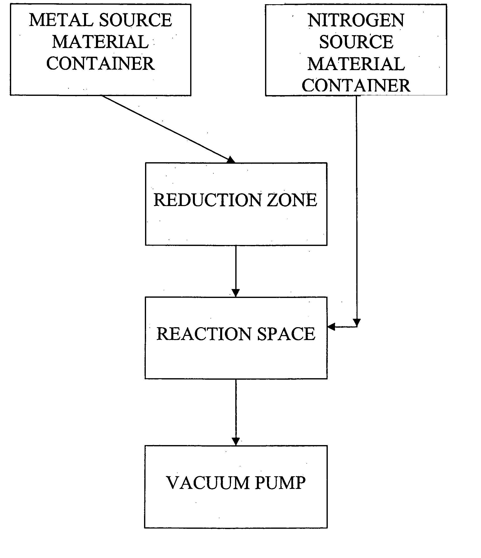
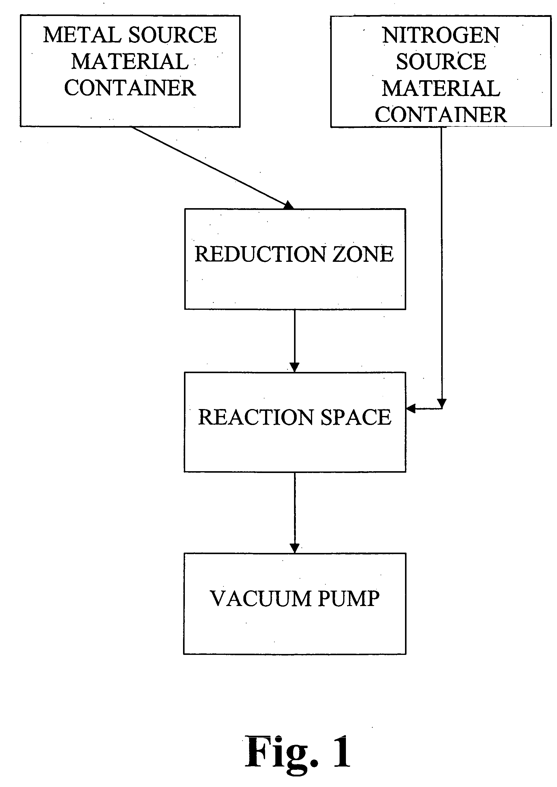
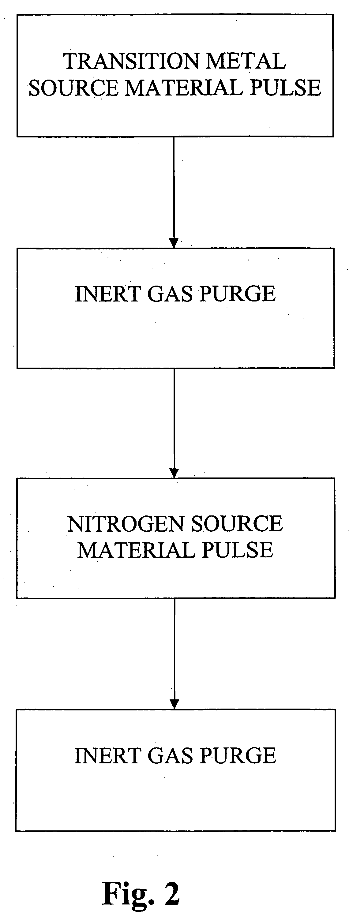
[0101] Experiments were performed with an F200 ALD reactor, as described in Finnish Patent No. 100409 of assignee by Suntola et al. Two series of titanium nitride samples were produced. One series of samples was made from TiCl4 and NH3. Heated reactor parts in contact with metal halides were passivated with amorphous aluminum oxide which protected the parts against corrosion. TiCl4 was evaporated from a source bottle at room temperature. The source gas was carried to the substrate chamber by nitrogen gas. Purging with nitrogen gas removed surplus TiCl4 molecules from the reactor. Then an NH3 gas pulse was introduced to the substrate chamber. The pulsing cycle was ended with a nitrogen purge which removed surplus NH3 and gaseous reaction byproducts from the reactor. The pulsing cycle was repeated 1000 times. The pressure of the substrate chamber was in the range of 200-1000 Pa. The resulting thin film on silicon wafer had metallic lustre with a yellowish hue. The growth rate at 400° ...

example 2

[0104] The same ALD reactor as in Example 1 was used for the reduction experiment. WF6 was evaporated from a source bottle at room temperature and carried towards the substrate chamber by nitrogen gas. In the gas flow channel near the substrate chamber there was tungsten metal foil heated to 400° C. WF6 flowed over tungsten metal, and the assumed reaction products (denoted with WFx) were carried to the substrate chamber by nitrogen gas. However, it was not possible to detect any visual signs of corrosion on W metal after the experiment. Theoretical calculations confirmed that at least simple reactions Eq. 3 and Eq. 4 are not favourable thermodynamically.

5WF6(g)+W→6WF5(g)ΔG(400° C.)=+1753 kJ  (Eq. 3)

2WF6(g)+W→3WF4(g)ΔG(400° C.)=−79 kJ  (Eq. 4)

theoretical example 3

[0105] Tungsten hexafluoride (WF6) is evaporated from the source bottle and carried towards the substrate chamber by nitrogen gas. Along the gas route there is a cartridge filled with tungsten silicide pieces. The cartridge is heated to 400° C. The reduction of WF6 into WF4 is thermodynamically favourable (Eq. 5). The pulsing sequence in the point of substrate is as follows: WFx vapor pulse / N2 gas purge / NH3 vapor pulse / N2 gas purge.

6WF6(g)+Wsi2(s)→7WF4(g)+2SiF4(g)ΔG(400° C.)=−737 kJ  (Eq. 5)

[0106] It can be argued whether SiF4 disturbs the thin film growth process. However, experiments with ALE have shown that it is very difficult to grow any silicon oxide or silicon nitride film from silicon halides. SiF4 molecules may have low reactivity with NH3 gas and they can be purged away with nitrogen.


PUM

PropertyMeasurementUnit
temperaturesaaaaaaaaaa
pressureaaaaaaaaaa
temperatureaaaaaaaaaa

Abstract

The invention concerns a method for modifying a source material used in an ALD process, a method for depositing transition metal nitride thin films by an ALD process and apparatus for use in such process. According to the present invention, transition metal source materials are reduced by vaporizing a metal source material, conducting the vaporized metal source material into a reducing zone comprising a solid reducing agent maintained at an elevated temperature. Thereafter, the metal source material is contacted with the solid or liquid reducing agent in order to convert the source material into a reduced metal compound and reaction byproducts having a sufficiently high vapor pressure for transporting in gaseous form.

Description

REFERENCE TO RELATED APPLICATIONS [0001] The present application claims priority under 35 U.S.C. §120 as a divisional of U.S. patent application No. 10 / 110,598, filed Apr. 11, 2002, which in turn is the U.S. national phase of international application number PCT / FI00 / 00884, filed Oct. 12, 2000 and claims priority under 35 U.S.C. §119 to Finnish application number 19992233, filed Oct. 15, 1999.BACKGROUND OF THE INVENTION [0002] 1. Field of the Invention [0003] The present invention relates to metal nitride thin films. In particular, the present invention concerns a method of in situ reduction of source chemicals as well as a method of growing of metal nitride thin films. The present invention also relates to an apparatus for growing thin films on a substrate by an ALD type process. [0004] 2. Description of the Related Art [0005] The integration level of components in integrated circuits is increasing, which rapidly brings about a need for a decrease of the size of components and inte...

Claims


Application Information

Patent Timeline
Patent Type & Authority Applications(United States)
IPC IPC(8): C23C16/32C23C16/34C23C16/448C23C16/44C23C16/455C30B25/02C30B29/02C30B29/36C30B29/38H01L21/285H01L21/768
CPCC23C16/32C23C16/34H01L2221/1078H01L21/76877H01L21/76843C23C16/44C23C16/4401C23C16/4488C23C16/45525C30B25/02C30B29/02C30B29/36C30B29/38H01L21/28568C23C16/45534H01L21/76856
Inventor ELERS, KAI-ERIK
Owner ELERS KAI ERIK
Why Eureka
Try Eureka