

Semiconductor device and manufacturing method thereof
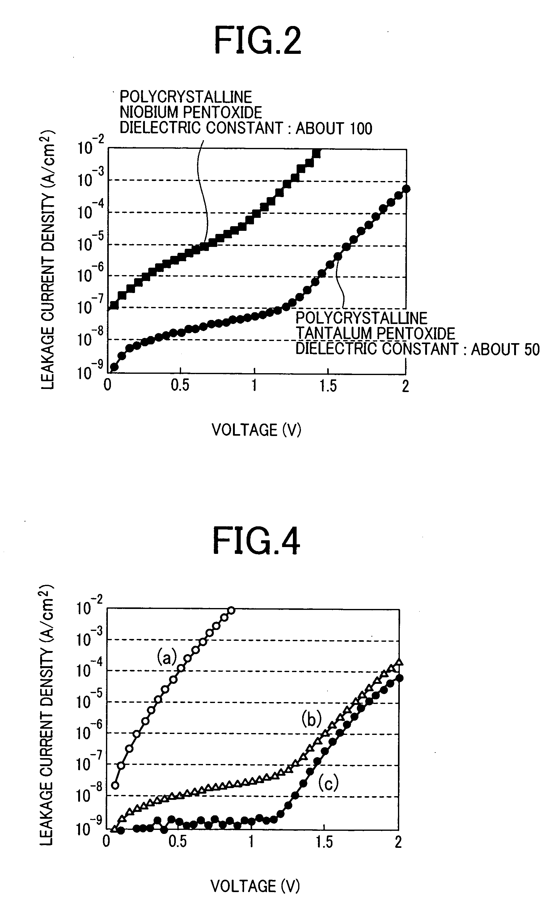
a semiconductor and semiconductor technology, applied in the direction of sidewalk paving, single unit paving, etc., can solve the problems of affecting electrical conductivity, reducing capacitor capacitance, adversely affecting electric conduction, etc., and achieves the effect of reducing leakage current, reducing leakage current, and overcoming large leakage current density
- Summary
- Abstract
- Description
- Claims
- Application Information
AI Technical Summary
Benefits of technology
Problems solved by technology
Method used
Image

Examples
embodiment 1
[0063] Embodiment 1
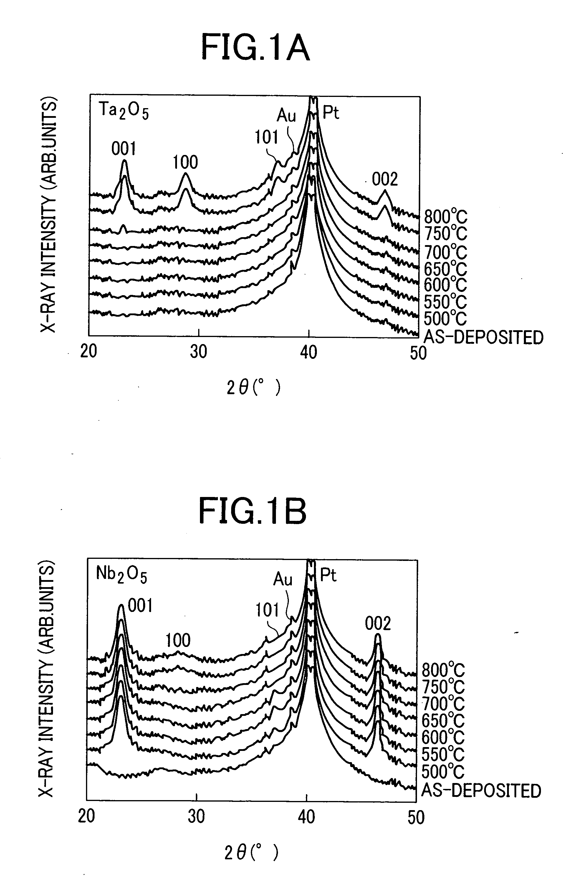
[0064] The embodiment 1 of the present invention will be described with reference to FIG. 5. The illustration is one, wherein this invention is applied to a semiconductor device, particularly to a DRAM, which has a MIM capacitor with a dielectric comprising a composite film of a polycrystalline niobium pentoxide and an amorphous tantalum pentoxide.
[0065] The following illustrates a method of manufacturing such a capacitor.
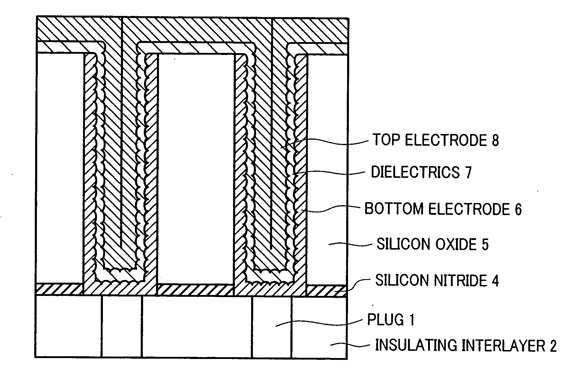
[0066] First of all, a silicon nitride film 4 and silicon oxide film 5 are formed on a substrate comprising plug 1 of polycrystalline silicon, barrier metal 2 of titanium nitride, and insulating interlayer 3 of a silicon oxide film. Subsequently, channels are formed in the silicon nitride film 4 and silicon oxide film 5 until the barrier metal 2 is exposed. The channels may be processed by a dry-etching method using a mask of photo-resist film or tungsten film.
[0067] Next is a process, wherein the bottom electrode 6 of ruthenium is deposited. ...
embodiment 2
[0083] Embodiment 2
[0084] The embodiment 2 of the present invention will be described with reference to FIG. 6. The illustration is one, wherein this invention is applied to a semiconductor device, particularly to a DRAM, which has a MIS capacitor using a dielectric comprising a composite film of a polycrystalline niobium pentoxide and an amorphous tantalum pentoxide.
[0085] The following illustrates a method of manufacturing such a capacitor.
[0086] First, a silicon nitride film 4 and a silicon oxide film 5 are formed on a substrate comprising plug 1 of polycrystalline silicon and insulating interlayer 3 of a silicon oxide film.
[0087] Subsequently, channels are formed in the silicon nitride film 4 and silicon oxide film 5 until the barrier metal 2 is exposed, as described in the embodiment 1.
[0088] Next is a process, wherein a 20 nm thick conductive amorphous silicon film is formed along the inner surface of the channel and the surface of the silicon oxide film 5, and the amorpho...
embodiment 3
[0095] Embodiment 3
[0096]FIG. 7 illustrates the cross section of a MISFET, a semiconductor device described in the embodiment 3. This is an embodiment, wherein a dielectric comprising a composite film of polycrystalline niobium pentoxide and amorphous tantalum pentoxide is applied to the gate insulator of a MISFET.
[0097] First, a silicon oxide film 11 is formed on the surface of a semiconductor substrate 9, channels 10 of the device separation area and inside the channels 10. Next is a process, wherein a composite film of niobium pentoxide and tantalum pentoxide is deposited. The deposition of the composite film is carried out under the same conditions as described in embodiment 1. Additionally, the film is heat-treated under the same condition as described in embodiment 1, forming a dielectric, wherein amorphous tantalum pentoxide is present along the grain boundaries of the polycrystalline niobium pentoxide. This dielectric will become a MISFET gate insulator as explained in the ...
PUM
| Property | Measurement | Unit |
|---|---|---|
| Fraction | aaaaa | aaaaa |
| Fraction | aaaaa | aaaaa |
| Thickness | aaaaa | aaaaa |
Abstract
Description
Claims
Application Information