Since production of a
single crystal substrate of the GaN semiconductor is difficult, there is a need to form a semiconductor apparatus using the GaN semiconductor on a substrate made of a different material.
Consequently, a good quality
crystal cannot be obtained when GaN is directly grown on
sapphire.
The
dislocation density of the GaN growth layer significantly restricts performance of a semiconductor apparatus to be produced from this, and moreover, there is a need to increase the amount of additive elements in the semiconductor layer for generation of sufficient carrier.
This has a problem of deteriorating a characteristic of a semiconductor apparatus, such as a life, a withstand
voltage, a driving
voltage, consumed
electric power (operation efficiency), an operation speed or a leak current.
Consequently, a lattice defect occurs on the interface even when GaN is grown on the
diboride single crystal substrate as described above, and a good quality
crystal cannot be obtained.
Moreover, differences in the coefficient of
thermal expansion between the above single
crystal substrates and the nitride semiconductor are large, and a difference in contraction amounts after
crystal growth at a high temperature of approximately 1000° C. causes cracks.
However, this technique has a problem that it is inferior in
mass production because it uses the MBE method.
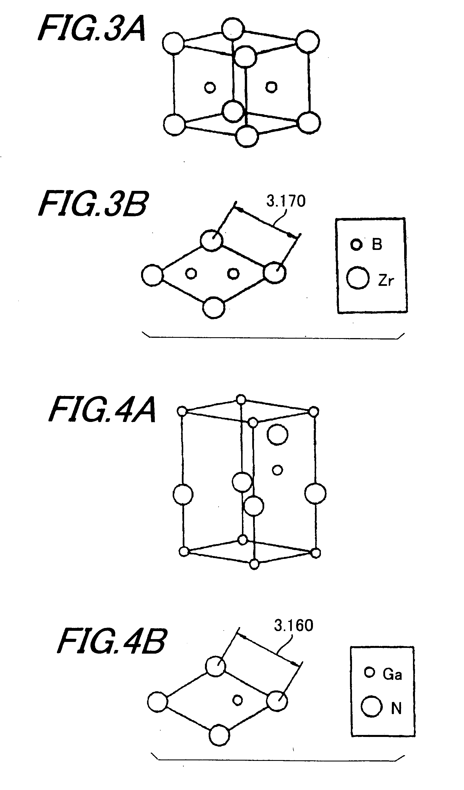
Further, in the prior art, a GaN film grown on the (0001) plane of a ZrB2
single crystal substrate by an MOVPE method has a problem that a
surface shape thereof tends to become uneven as shown in FIG. 13.
However, according to both the techniques, in the GaN film grown on the (0001) plane of the ZrB2
single crystal substrate, a
rocking curve half value width of (0002) plane
omega scan by an X-
ray diffraction method, which becomes an indicator of evaluation of quality, is approximately 1000 seconds, which is not sufficiently good (refer to “Study on the
crystal growth and properties of group-III
nitride semiconductors on ZrB2 substrate by metalorganic
vapor phase epitaxy” master's thesis written by Yohei Yukawa, graduate school of Meijo University, 2001).
Still further, a
band gap of AlN is as large as 6.2 eV, and therefore, it is difficult to decrease resistance by
doping.
Up to now, there is no substrate that achieves a lattice match with the nitride semiconductor.
However, for example, regarding the
sapphire substrate and GaN, a ratio of
lattice mismatch is 13.8% and a difference in the coefficient of
thermal expansion is 3.2×10⁻⁶ / K, and there is a problem resulting from the mismatch such that dislocations of 108 to 1010 cm−2 arises in the GaN film because of a crystal defect caused on an interface between the
sapphire substrate and the GaN film.
Further, because of the defect and
thermal distortion, the GaN film is warped, and crystalline quality is significantly deteriorated.
Furthermore, considering production of a device such as a
laser diode, the nitride semiconductor is formed on a substrate made of a material of different kind from the nitride semiconductor such as GaN and the like, and therefore, there arises such a problem that, in the case of forming a reflection surface of a laser
resonator, cleaved planes of the substrate made of a material and the nitride semiconductor are different, and that formation by cleavage is difficult.
However, regarding the nitride semiconductor such as GaN, a
melting point is high and a dissociation pressure of nitride is high at the
melting point, and therefore, production of a bulk single crystal is difficult.
However, in the step of separating the substrate and the nitride semiconductor in the aforementioned production method, a method of abrading the substrate arises a problem that stress from the nitride semiconductor thick film becomes large as the substrate becomes thin, and that the stress acts on the substrate, thereby worsening a warp thereof and causing cracks.
However, according to this method, only a small part of the interface is separated because an area irradiated is small, and stress concentrates on a small attaching part, with the result that cracks are caused.
Moreover, since the area irradiated is small, a time period for treatment is long.
However, since SiO2 is filled in, it is difficult to carry out
mask treatment on SiO2.
Moreover, since curved dislocations concentrate on a central portion on the SiO2 line, there arises a problem of inclination of
crystal orientation in a horizontal direction of the substrate, for example.
In addition, the ELO growth method needs a complicated production process, and therefore, brings about cost increase.
As described above, according to the conventional production methods, when the substrate made of a material of different kind from nitride semiconductor and the nitride semiconductor thick film are separated, stress resulting from differences in lattice constants and the coefficient of
thermal expansion causes a warp and cracks on the produced nitride semiconductor apparatus.
Moreover, the production process is complicated in the ELO growth that reduces dislocations, and it is difficult to keep away from a portion on the which penetration
dislocation density concentrates, and to carry out the
mask treatment on contained SiO2.
Furthermore, there arises a problem of inclination of
crystal orientation in a horizontal direction of the substrate because of curved
dislocation, for example.

