Apparatus and processes for the mass production of photovoltaic modules

a photovoltaic module and photovoltaic technology, applied in the direction of crystal growth process, polycrystalline material growth, chemically reactive gas, etc., can solve the problem of low throughput, low throughput, and the quantity of material which can be lawfully released into the environment or into the occupational setting, and achieve low resistance ohmic contact, high throughput rate, and stable over time

Inactive Publication Date: 2005-07-21
COLORADO STATE UNIVERSITY
View PDF1 Cites 70 Cited by
  • Summary
  • Abstract
  • Description
  • Claims
  • Application Information

AI Technical Summary

Benefits of technology

[0021] Another aspect of the present invention is a novel vacuum process to produce a p+ ohmic contact region by subliming a metal salt onto a CdTe layer. Our ohmic contact formation process has the advantage of producing, at high throughput rates, a low resistance ohmic contact that is stable over time.
[0022] Another aspect of the present invention is a unique high throughput, low cost spray process to form the back electrode. This process has the advantage of producing a durable, high conductivity back electrode using known low cost industrial spray methods.
[0023] Another aspect of the present invention is to provide novel high throughput, low cost processes to perform module scribing using abrasive blasting or mechanical brushing through a mask. These novel scribing processes have the advantage of selectively scribing the semiconductor layers without scribing the TCO layer. In addition, the scribe process may be adjusted so that the TCO layer may be removed as well.
[0024] Another aspect of the present invention is a novel vacuum process station to selectively heat substrates and films, to expose substrates and films to vapor, to deposit thin films on a substrate, and to strip thin films off of a substrate. This vacuum process station allows substrates to be transported into and out of vacuum. When used as a deposition source, our vacuum process station has the advantage of very minimal vapor leakage, which significantly reduces occupational exposure to toxic materials. This unique deposition source deposits very uniform layers and is suitable for long term continuous operation.
[0025] Another aspect of the present invention is a novel substrate transport apparatus, which is employed to move substrates within vacuum or, in combination with a unique opening, to transport substrates rapidly into and out of vacuum. This substrate transport apparatus is robust, simple, and low cost and has the additional advantage of not collecting any coatings as it moves substrates through the thin film deposition processes.
[0026] Yet another aspect of the present invention is to provide substrate cleaning in a clean mini-environment at the entrance to the inline continuous vacuum process, which has the advantage of greatly reduced cost resulting from the elimination of a clean room to contain the entire process line.

Problems solved by technology

To date, no technology suitable for commodity level manufacturing of CdTe PV modules has been developed, thus demonstrating the need for innovation in this area.
Vacuum deposition methods for other thin film PV devices require costly, complex high vacuum equipment and results in low throughput.
According to U.S. government regulations, the quantity of this material which can be lawfully released into the environment or into an occupational setting is extremely small.
All of the prior art methods for the production of CdTe modules have limitations that render them unsuitable for commodity level manufacturing.
These batch type processes are inefficient and involve extremely high costs in order to increase throughput to the commodity manufacturing level.
Prior art metallization steps also exhibit low throughput and require costly process equipment.
Known laser scribing methods used in the PV industry are associated with low production speed and high capital cost.
The entire VTD method is very complex and costly.
The heated vessels of this method contain toxic vapors, which pose significant occupational safety problems when they are opened for reloading during processing.
These nano-particles degrade the film qualities and lead to occupational hazards when the system is serviced.
Any CdS or CdTe vapors that are carried past the substrate will be wasted.
Any deposits of waste material on the inner surface of the vacuum chamber, pumps, exhaust, etc. must be cleaned, thereby exposing maintenance workers to toxic materials and raising occupational safety issues.
This wastes energy and increases the capital costs.
Other processing steps, such as the CdCl2 treatment, ohmic contact formation, and metallization are inherently low throughput batch processes.
Scribing is taught to be either laser scribing or photolithography, both of which are slow and costly processes.
As described above, known methods for performing these steps have limitations.
However, it is not clear if long term operation and uniformity of deposition over time and across large substrates are achieved.
It is the present inventors' experience that this gap and the associated vapor leak causes non-uniform deposition on the substrates and also results in condensation of toxic materials on unwanted areas on the inner surfaces of the process chamber.
However, higher pressures lead to lower deposition rates and greater nano-particle formation.
These very small particles degrade film quality and pose a health hazard to workers during routine maintenance inside the vacuum chamber.
In addition, nothing in the prior art describes an overall process to perform the series of steps of substrate heating, depositing an n-type CdS layer, depositing a p-type CdTe layer, performing a CdCl2 treatment, and forming an ohmic contact inline, continuously, and in one vacuum boundary.
The apparatuses described in the prior art simply do not meet these requirements.

Method used


Image

  • Apparatus and processes for the mass production of photovoltaic modules
  • Apparatus and processes for the mass production of photovoltaic modules
  • Apparatus and processes for the mass production of photovoltaic modules

Examples


Embodiment Construction

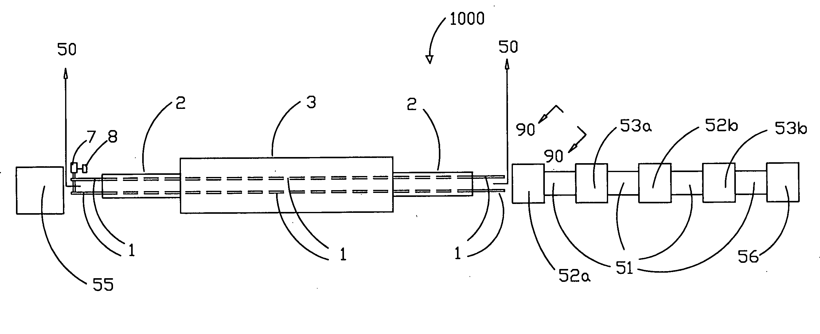
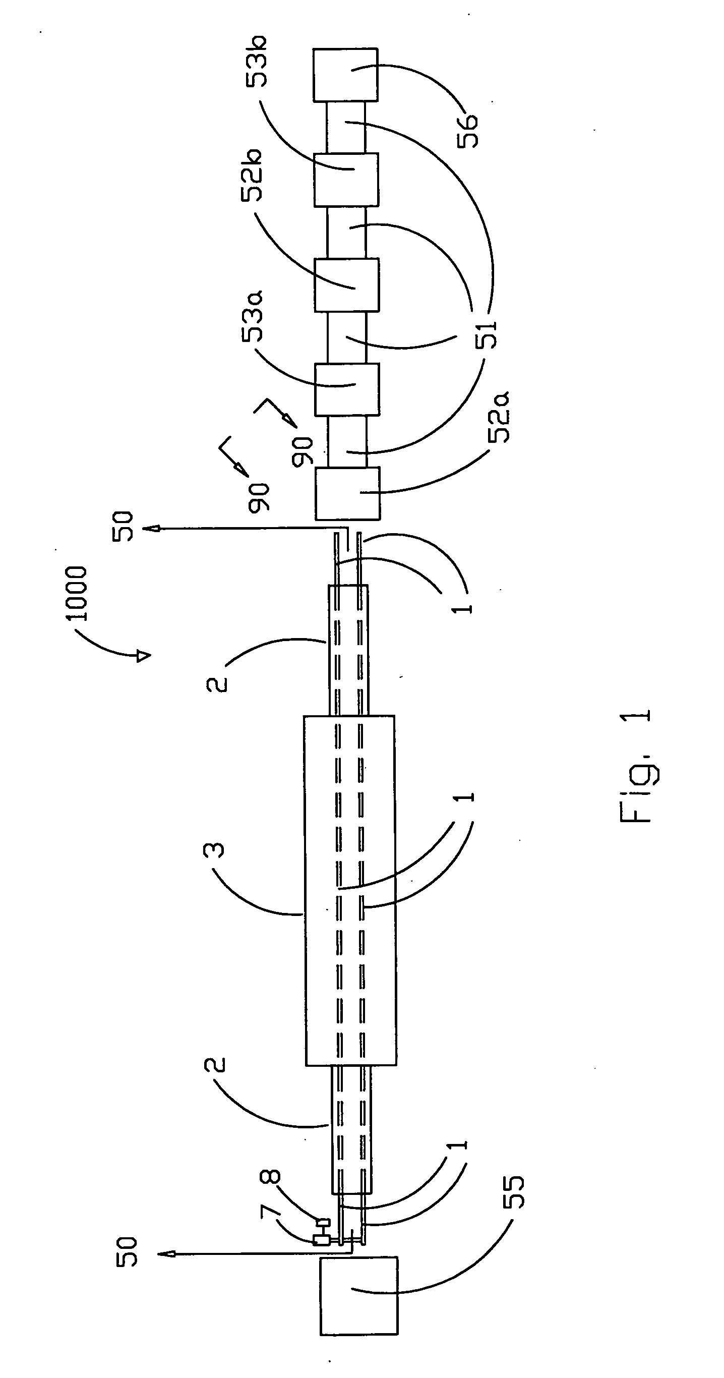
[0041] Referring now to FIG. 1, there is shown an overview of the preferred embodiment of an apparatus 1000 for producing photovoltaic modules in accordance with the present invention. A substrate cleaning station 55 cleans the commercially available substrates that typically comprise low cost soda lime glass coated with transparent conducting oxide (TCO). After cleaning, a pair of metal strip belts 1 transport the substrates through the next portion of the apparatus 1000. The belts may be moved bidirectionally by means of a known stepper motor 7. Precise indexing of the position of the pair of belts 1 is accomplished by the use of a commercially available stepper motor controller 8. The pair of metal strip belts 1 pass through a pair of openings 2 and a vacuum chamber 3. A plurality of process stations for the processing of the critical semiconductor layers are contained within the vacuum chamber 3, and are described in detail below. Another series of process stations are linked by...


PUM

PropertyMeasurementUnit
operating pressureaaaaaaaaaa
lengthaaaaaaaaaa
distanceaaaaaaaaaa

Abstract

An apparatus and processes for large scale inline manufacturing of CdTe photovoltaic modules in which all steps, including rapid substrate heating, deposition of CdS, deposition of CdTe, CdCl2 treatment, and ohmic contact formation, are performed within a single vacuum boundary at modest vacuum pressures. A p+ ohmic contact region is formed by subliming a metal salt onto the CdTe layer. A back electrode is formed by way of a low cost spray process, and module scribing is performed by means of abrasive blasting or mechanical brushing through a mask. The vacuum process apparatus facilitates selective heating of substrates and films, exposure of substrates and films to vapor with minimal vapor leakage, deposition of thin films onto a substrate, and stripping thin films from a substrate. A substrate transport apparatus permits the movement of substrates into and out of vacuum during the thin film deposition processes, while preventing the collection of coatings on the substrate transport apparatus itself.

Description

GOVERNMENT SUPPORT [0001] This invention was made with Government support under grants awarded by the National Science Foundation and the Department of Energy. The Government has certain rights in this invention.FIELD OF THE INVENTION [0002] The present invention relates to apparatus and processes for the mass production of low cost photovoltaic modules and, more specifically to an inline continuous vacuum apparatus and process for fabricating the critical semiconductor layers, which together with attendant non-vacuum processes, are all accomplished at high throughput. BACKGROUND OF THE INVENTION [0003] Photovoltaic (PV) modules are used to generate electricity from sunlight by the photovoltaic effect. It has been recognized for decades that if these modules could be mass produced at low cost, they could be used to meet a considerable portion of the world's energy needs. Major companies, such as Royal Dutch / Shell and BP-Amoco, have stated that PV modules have the potential to become...

Claims


Application Information

Patent Timeline
Patent Type & Authority Applications(United States)
IPC IPC(8): H01L21/365H01L21/203H01L31/04H01L31/18
CPCY02E10/543H01L31/1828
Inventor BARTH, KURT L.ENZENROTH, ROBERT A.SAMPATH, WALAJABAD S.
Owner COLORADO STATE UNIVERSITY
Why Eureka
Try Eureka