Stackable optoelectronics chip-to-chip interconnects and method of manufacturing

a technology of optoelectronics and chip-to-chip interconnection, applied in sustainable manufacturing/processing, semiconductor/solid-state device details, instruments, etc., can solve the problems of increasing the difficulty of interconnection on the printed circuit board (pcb), noise from off-chip electrical signals, and achieving higher data rates. , to achieve the effect of reducing the skew of signal interconnection

Active Publication Date: 2005-10-13
BANPIL PHOTONICS
View PDF5 Cites 142 Cited by
  • Summary
  • Abstract
  • Description
  • Claims
  • Application Information

AI Technical Summary

Benefits of technology

[0028] Other object of this invention is to minimize the skew in the signal interconnection, o

Problems solved by technology

Simultaneously achieving higher data rates and higher interconnect densities within the higher level of packaging, covering from die-level packaging to chip-to-chip (hereafter chip indicates the die with package) interconnection on the printed circuit board (PCB), will be increasingly difficult as the IC technologies continue to evolve increasing the signal speed and interconnection number.
This off-chip electrical signal creates noises such as reflection caused by poor shapes of electrical interconnects, connecting the inter chip, or the influence of the cross-talk.
In addition, the high-speed signal creates also high frequency electromagnetic waves from the electric interconnect to adversely affects the peripheral circuits.
In the case of high speed off-chip interconnects especially over 3 GHz where line length is long, both reducing reflection loss and also suppressing electromagnetic interference are practically challenging in some extent, and are not cost-effective to implement by using of conventional PCB technology.
In this case, the fully integration technology within IC in other words, the intra chip signal speed is not fully utilized.
However, if this technique is used in off-chip interconnections where chip-to-chip distance is few centimeters, this technique will be make the whole interconnection bulky, and could not be used in practical application where existing chip package and conventional PCB technology are frequently used.
However, in an application where existing chip with package such as BGA and CSP are used, the use of this free-space optic concept makes the interconnects more bulky, and miniaturization is difficult to achieve.
Furthermore, free space optics concept is also not friendly to implement in the electronics systems such as desktop computer and video-gaming

Method used


Image

  • Stackable optoelectronics chip-to-chip interconnects and method of manufacturing
  • Stackable optoelectronics chip-to-chip interconnects and method of manufacturing
  • Stackable optoelectronics chip-to-chip interconnects and method of manufacturing

Examples


first embodiment

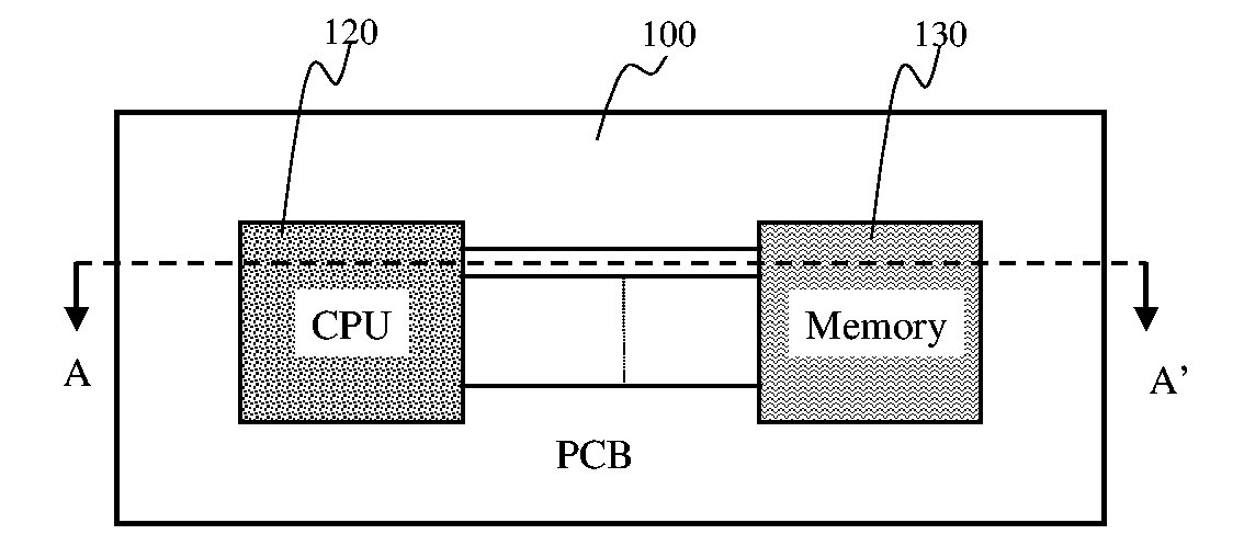
[0089] An important point of optical interconnects system for high speed off-chip connection is the idea that essential part, an optical-electrical (hereafter mentioned as “O-E”) board is required and it is to be compatible and easily stackable with the available chip package and also PCB. To make the cost-effective, the board should be friendly for the manufacturing as the electronics components.

[0090] In off-chip interconnection, the signal between the chips may be conveyed electrically through the wire or optically through the optical media. Especially, the idea is to transfer the high-speed signal from one chip to another after conversion into optical from electrical and vice-versa for the receiving signal. The low speed signal connection and the rest of the others connection such as ground and power line connections are done through the electrical wire. When the signals are conveyed by light (i.e. optically), the optoelectronics devices provide the conversions between the ligh...

second embodiment

[0095]FIG. 6 is a plan view, showing from the optical part mounting side (bottom), the O-E board 140 according to the The O-E board 140 for interconnects is included a singulated chip (with package) 120 and a singulated portion of the circuit 152. The O-E board 140 and the circuit 152 have peripheral outline substantially similar to that of the package 120. The circuit 152 includes a substrate 150, which comprises with insulating, flexible material or rigid material. The flexible material could be any kinds of polymer material, which includes polyimide, polyester, epoxy, urethane, polystyrene, silicon or polycarbonate. The substrate 152 also includes the rigid substrate. Suitable materials for the rigid substrate cover ceramic materials including aluminum nitride, aluminum oxide, and boron nitride. The material having high thermal conductivity and high dielectric constant also covers this substrate material. The thickness for the substrate 152 can be 20 to 500 um.

[0096] The circuit...


PUM


Abstract

An optoelectronics chip-to-chip interconnects system is provided, including packaged chips to be connected on printed-circuit-board (PCB), multiple-packaged chip, optical-electrical(O-E) conversion means, waveguide-board, and PCB. Single to multiple chips interconnects can be possible using this technique. The packaged-chip includes semiconductor-die and its package based on the ball-grid array or chip-scale-package. The O-E board includes the optoelectronics components and multiple electrical contacts. The waveguide board includes electrical conductors transferring signal from O-E board to PCB and the flex optical waveguide easily stackable onto the PCB, to guide optical signal from one chip-to-other chip. The chip-to-chip interconnects system is pin-free and compatible with the PCB. The main advantages are that standard packaged-chip and conventional PCB technology can be used for low speed electrical signal connection. Also, the part of the heat from the packaged chip can be transmitted to PCB through conductors, so that complex cooling system can be avoided.

Description

CROSS REFERENCE TO RELATED APPLICATIONS [0001] This application claims the benefits of U.S. Provisional Application No. 60 / 521,153 filed Feb. 27, 2004.FIELD OF THE INVENTION [0002] This invention relates to chip-to-chip interconnection, and more particularly to, connecting electrical signal line of single or multiple processor-chips to signal line of single or multiple memory chips, used in all kinds of computers covering from personnel computer to super-computer, and also in game system. BACKGROUND OF THE INVENTION [0003] The increasing of higher level of integration within electrical integrated circuit (IC) leads to both higher data rates and larger number of IC interconnections. Today, the inherent signal speed of IC is increased to 3 GHz, and shortly it will be reached to over 10 GHz. The number of pin connection is also increased, with single IC requiring close to 2000 interconnection (i.e. single processor), and shortly it will be increased to over 5000. Simultaneously achievi...

Claims


Application Information

Patent Timeline
IPC IPC(8): G02B6/42H01L23/02G02B6/12G02B6/43H05K1/02H05K1/18H05K1/14
CPCG02B6/12002G02B6/4214Y02P70/611H01L24/48H01L2924/10329H01L2924/1432H01L2924/1434H01S5/183H05K2201/10121G02B6/43H01L2224/16H01L2924/01046H01L2924/01078H01L2924/01079H01L2924/09701H01L2924/3011H01L2924/3025H05K1/0274H05K1/141H05K1/181H05K2201/10734G02B6/122H01L2924/00014H01L2224/05573H01L2224/05568G02B2006/12147H01L2924/1461H01L2924/12043H01L2924/12042G02B6/4224G02B6/32H01S5/02272H01S5/02248H05K1/144H01L2924/10335H05K2201/10515H01L2224/48227H01L2224/48106H01L2224/48091H01L2224/16238H01L25/167H01L24/49H01L24/17G02B6/428G02B6/4279G02B6/4268G02B6/4257H01L2924/00H01L2224/05599H01L2224/45099Y02P70/50H01S5/0237H01S5/02325
Inventor DUTTA, ACHYUT KUMAR
Owner BANPIL PHOTONICS
Why Eureka
Try Eureka