Semiconductor substrate, semiconductor device, and manufacturing methods for them

a semiconductor and substrate technology, applied in the direction of semiconductor devices, identification means, instruments, etc., can solve the problems of insufficient device performance and integration, inability to adopt transistors for integration of complex systems, and difficulty in ensuring high-speed performance and high integration density, etc., to achieve the effect of reducing the area of the device, and improving the performan

Inactive Publication Date: 2005-11-03
SHARP KK
View PDF16 Cites 30 Cited by
  • Summary
  • Abstract
  • Description
  • Claims
  • Application Information

AI Technical Summary

Benefits of technology

[0031] With this arrangement using a singlecrystalline Si, the resulting semiconductor device is superior in performance and less varied in characteristic.
[0032] Further, in this structure not providing a conventional well, a channel stop, or a well-contact, the area of the device area is reduced, allowing more dense integration, thereby realizing a highly-dense semiconductor substrate. Further, since the conventional well is omitted, the device may be made thinner than the conventional structure using a well. Thus, the semiconductor element can be made as a thin film which can coexist with the TFTs formed from other polycrystalline Si upon formation of the semiconductor device, allowi

Problems solved by technology

However, in such a display device, like a liquid crystal display device or an OLED (Organic Light Emitting Diode: organic EL) using a large glass substrate, there is some problems in using a driver IC including a transistor made of a non-singlecrystalline Si, particularly a poly-Si, because of the variation in characteristics due to the particular crystal grain boundaries of poly-Si and poor quality of gate insulating film, thereby disabling the transistor to be adopted for integration of a complex system.
Particularly, when a highly-integrated semiconductor device is directly mounted to a display substrate, or on systematization thereof, there are difficulties to ensure high-speed performance and high integration density because of insufficiencies in driving speed, micro fabrication, and device performance (mobility, control of the threshold, sharpness of transmission characteristic).
The foregoing structure is therefore insufficient in device performance and integration density to realize a desired system integration in a driving system used for an image processor or a timing controller, which requires a superior-performance.
Accordingly, there is a serious difficulty in fabrication of pixel TFTs and a high-performance/high-density driver for driving the pixel TFTs directly onto a large display substrate, of a glass or the like.
However, the trend of miniaturization of transistor arises a new problem regarding the area for device isolation.
Thus, to reduce the area for device isolation, retrograde well (reverse-impurity concentration gradient-well) structure or the like has been introduced; however, this structure requires ion implantation many times and makes the process complicated, thus causing a cost rise and a decrease i

Method used


Image

  • Semiconductor substrate, semiconductor device, and manufacturing methods for them
  • Semiconductor substrate, semiconductor device, and manufacturing methods for them
  • Semiconductor substrate, semiconductor device, and manufacturing methods for them

Examples


referential embodiment

[0063] Before the explanation of the present embodiment, the following describes a technology suggested in an unpublished patent application, which is made by the same inventor prior to the present invention, aimed at solving the conventional problems.

[0064] First, the conventional problems are summarized below.

[0065] In a SOI (Silicon On Insulator) structure, since the devices are formed on a silicon (Si) wafer, the total size of all devices to be provided thereon needs to fall within the silicon (Si) wafer. However, the size of silicon (Si) wafer is limited, and may be smaller than a large glass substrate.

[0066] Moreover, since a singlecrystalline Si device formed on the silicon (Si) wafer is bonded onto a glass substrate with an adhesive of, for example, an epoxy resin, there are serious difficulties to additionally performing a defect recovery thermal process (Annealing process), an inter-layer insulating film forming process, or a metal-wiring forming process, after the bond...

first embodiment

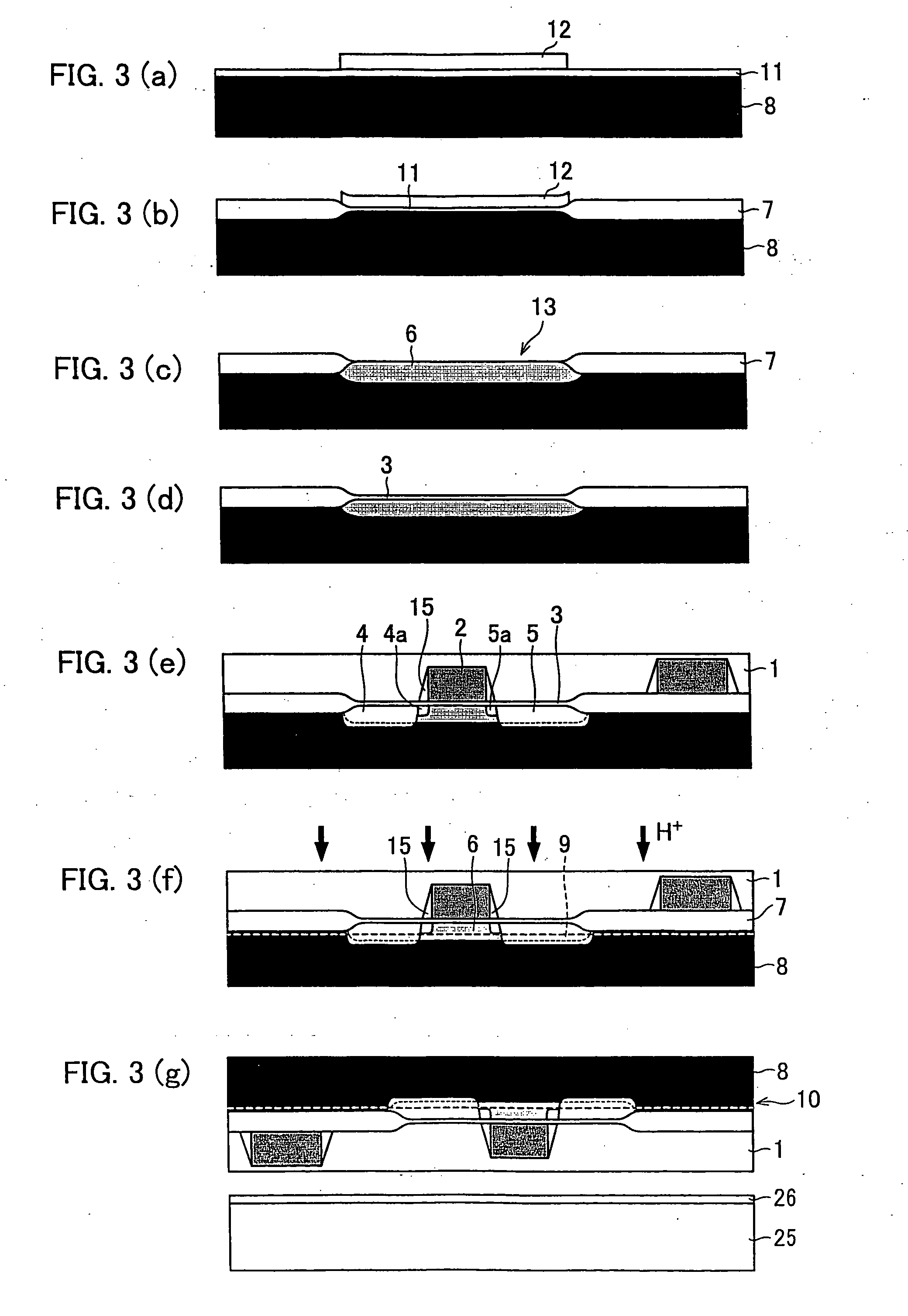
[0077] One embodiment of the present invention is described below with reference to FIGS. 1 through 7.

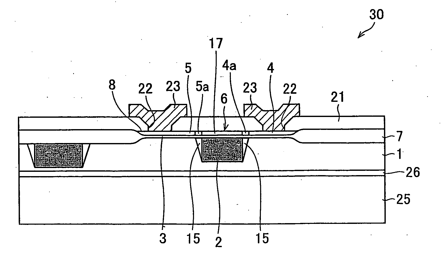
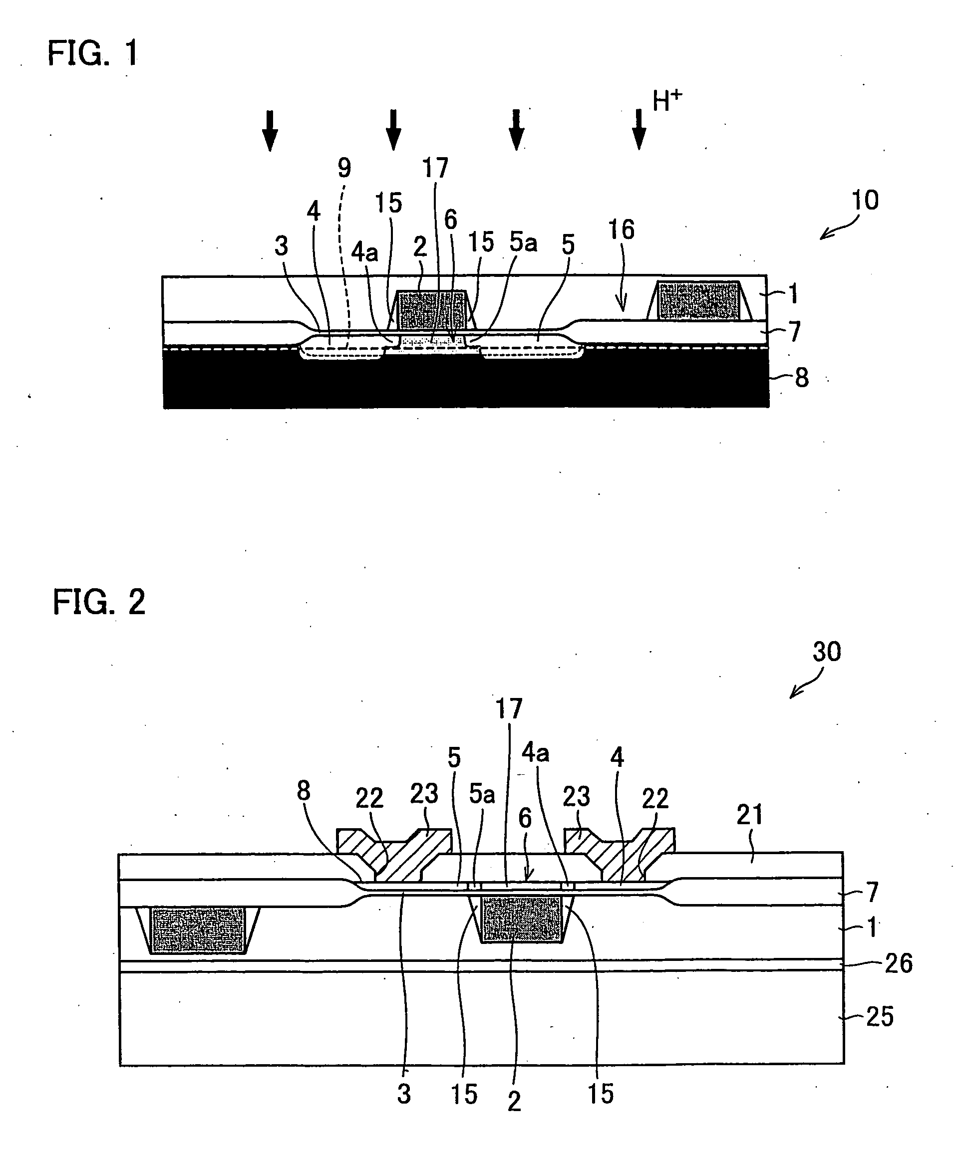
[0078] Note that, the semiconductor substrate and the semiconductor device according to the present embodiment provide improved performance and improved functionality on account of a structure in which a MOS non-singlecrystalline Si thin film transistor and a MOS singlecrystalline Si thin film transistor are formed in different regions of an insulating substrate, such as a glass substrate. This semiconductor device is to be mounted to an active matrix substrate using TFTs (Thin Film Transistor).

[0079] The MOS thin film transistor is a general transistor comprising an active layer, a gate electrode, a gate insulating film, and a high concentration impurity doped portion (source / drain electrodes) formed on each side of the gate, wherein the gate electrode controls the carrier density of the semiconductor layer under the gate, so as to control a flow of source-drain current.

[0080] A...

second embodiment

[0144] Another embodiment of the present invention is explained below with reference to FIGS. 8 through 11. Note that, the following embodiment is identical to First Embodiment except for the arrangements explained below. For ease of explanation, materials having the equivalent functions as those shown in the drawings pertaining to the foregoing First Embodiment will be given the same reference symbols, and explanation thereof will be omitted here.

[0145] In the semiconductor substrate 10 and the semiconductor device 30 according to First Embodiment, as shown in FIG. 2, the metal wiring layers 23 as external electrodes are connected directly to the source and drain regions 4 and 5 through contact holes 22 of the protective-insulating-interlayer film 21.

[0146] On the other hand, as shown in FIG. 8, in the semiconductor device 50 according to the present embodiment, the first metal wiring 42, which is the first wiring layer for making conduction with the source / drain region 4 / 5, is f...


PUM


Abstract

The present invention provides a semiconductor substrate, which comprises a singlecrystalline Si substrate which includes an active layer having a channel region, a source region, and a drain region, the singlecrystalline Si substrate including at least a part of a device structure not containing a well-structure or a channel stop region; a gate insulating film formed on the singlecrystalline Si substrate; a gate electrode formed on the gate insulating film; a LOCOS oxide film whose thickness is more than a thickness of the gate insulating film, the LOCOS oxide film being formed on the singlecrystalline Si substrate by surrounding the active layer; and an insulating film formed over the gate electrode and the LOCOS oxide film. On this account, on fabricating the semiconductor device having a high-performance integration system by forming the non-singlecrystalline Si semiconductor element and the singlecrystalline Si semiconductor element on the large insulating substrate, the process for making the singlecrystalline Si is simplified. Further, the foregoing arrangement provides a semiconductor substrate and a fabrication method thereof, which ensures device isolation of the minute singlecrystalline Si semiconductor element without highly-accurate photolithography, when the singlecrystalline Si semiconductor element is transferred onto the large insulating substrate.

Description

[0001] This Nonprovisional application claims priority under 35 U.S.C. § 119(a) on Patent Application No. 2004 / 93694 filed in Japan on Mar. 26, 2004, the entire contents of which are hereby incorporated by reference. FIELD OF THE INVENTION [0002] The present invention relates to a semiconductor substrate and a semiconductor device used for an active matrix liquid crystal display device that is driven by TFTs (Thin Film transistor), such as a high-functional liquid crystal display device, an OLED (Organic Light Emitting Diode: Organic EL) display device or the like, in which the peripheral circuits, the control circuit, the MPU (Micro Processing Unit), and / or the image processing circuit are all integrated into a single substrate. The present invention also provides fabrication method for the semiconductor substrate / device. [0003] The present invention particularly relates to a system-on-panel technology that offers great improvement of circuit performance with the use of singlecryst...

Claims


Application Information

Patent Timeline
IPC IPC(8): G02F1/136G02F1/1368G09F9/30G09G3/00H01L21/00H01L21/02H01L21/316H01L21/336H01L21/469H01L21/76H01L21/762H01L21/77H01L21/8234H01L21/8238H01L21/84H01L27/08H01L27/088H01L27/092H01L27/10H01L27/12H01L29/00H01L29/786
CPCH01L21/76202H01L21/76254H01L27/1203H01L29/78609H01L27/1266H01L29/78603H01L27/1214H01L21/18
Inventor TAKAFUJI, YUTAKAFUKUSHIMA, YASUMORIMORIGUCHI, MASAO
Owner SHARP KK
Why Eureka
Try Eureka