Semiconductior multilayer structurehaving inhomogeneous quantum dots, light-emitting diode using same, semiconductor laser diode, semiconductor optical amplifier, and method for manufacturing them
- Summary
- Abstract
- Description
- Claims
- Application Information
AI Technical Summary
Benefits of technology
Problems solved by technology
Method used
Image

Examples
example 1
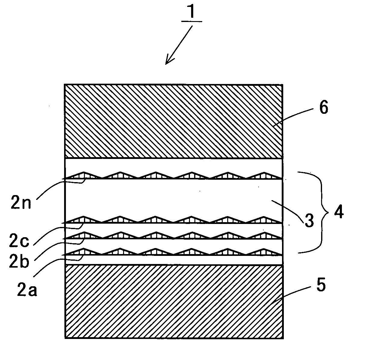
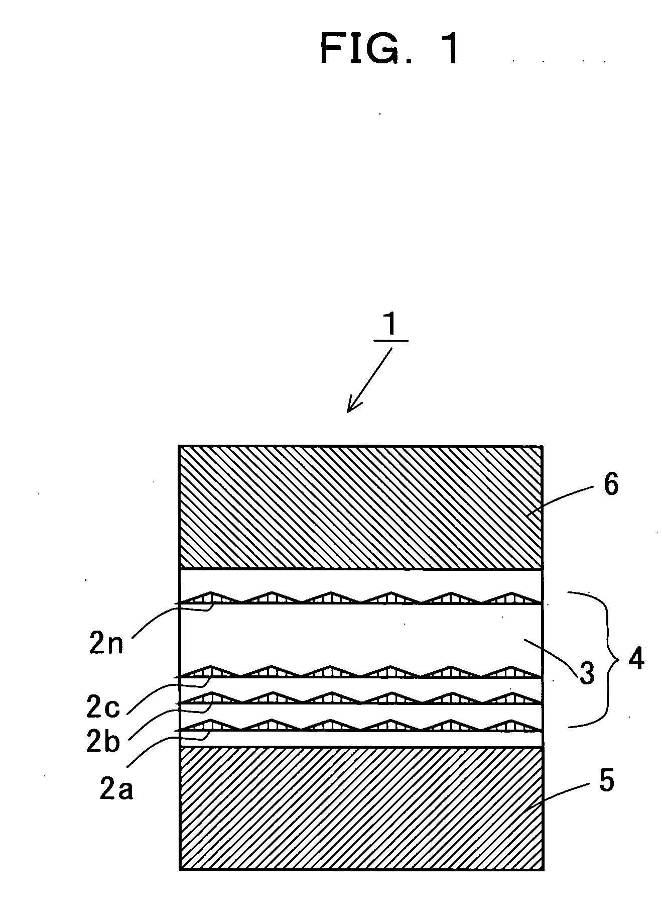
[0151] Firstly, a specific example is given of the semiconductor multi-layered structure 1 using a non-uniform quantum dot structure that can be formed without lattice strain, which was fabricated using MOCVD and droplet epitaxial growth process. For MOCVD, use was made of an apparatus as described above in connection with FIG. 12.
[0152] After cleaning with an organic solvent and etching with an acidic etching liquid, an n-type InP substrate 52 having a thickness of 350 μm and an electron concentration of 4×1018 cm−3 and with a (100) plane was introduced from the specimen loading chamber 55 into the silica reaction tube 51 and set in position on the susceptor 53 therein. The silica reaction tube 51 was then evacuated to vacuum at a selected pressure by the vacuum pumping unit 60, followed by passing purified hydrogen gas 73 to flow through the silica reaction tube 51 which was then maintained at a pressure of 76 Torr.
[0153]FIG. 13 shows graphs illustrating a relationship between t...
example 2
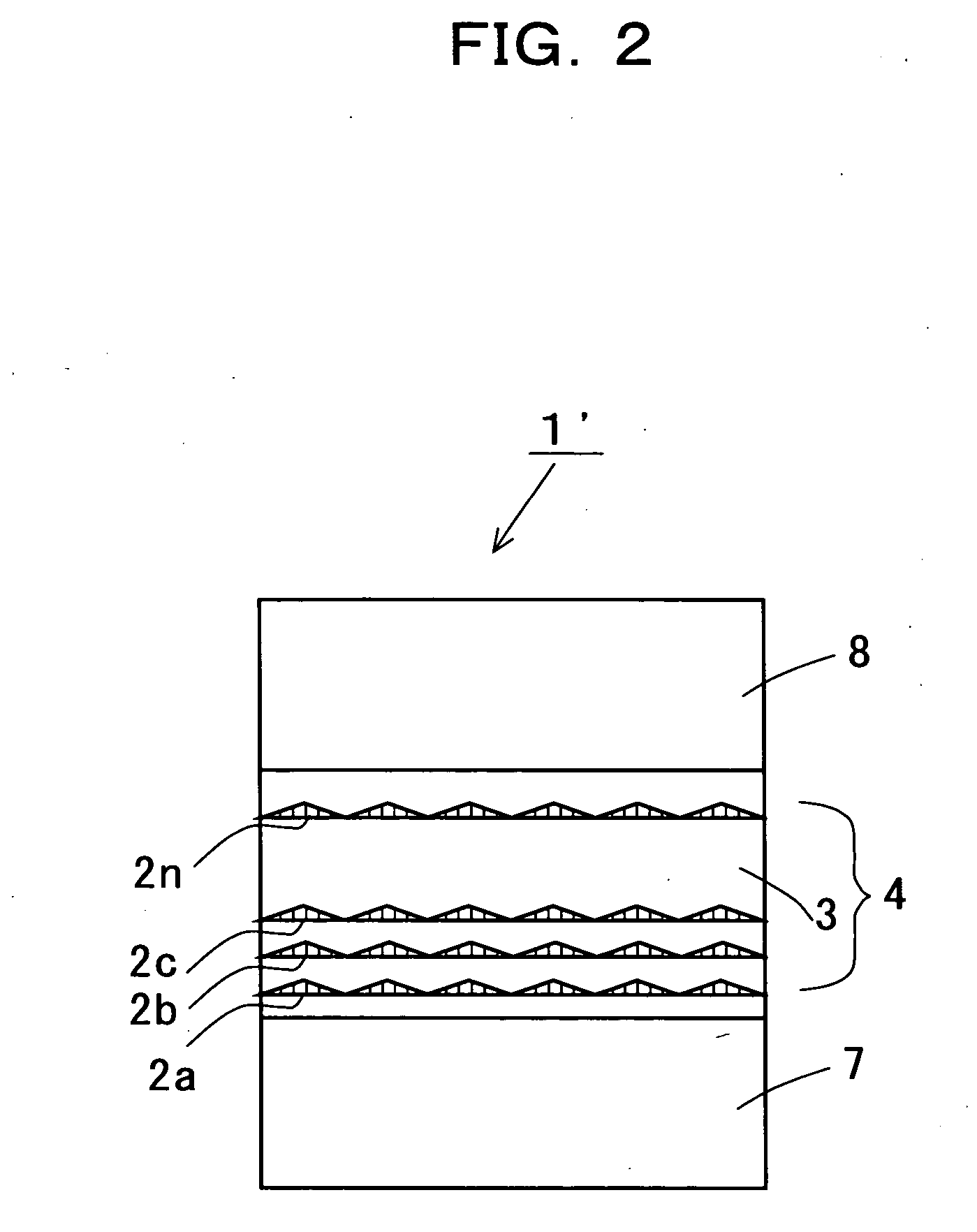
[0161] A specific example is given of crystal growth for an LED 15 using a semiconductor multi-layered structure having non-uniform quantum dots as shown in FIG. 5. Here, use was made of the same MO CVD apparatus shown in and described in connection with FIG. 12.
[0162] The multi-layered structure of an LED 15 was formed by depositing an n-type semiconductor layer 7 of InP with an impurity density of 1×10¹⁷ to 5×1018 cm−3 to a thickness of 0.001 μm to 2 μm, an active layer 4 having non-uniform quantum dots formed without requiring lattice strain to a thickness of 0.1 μm to 3 μm, and a p-type semiconductor layer 8 of p-type InP with an impurity density of 1×10¹⁸ to 5×1019 cm−3 to a thickness of 0.5 μm to 5 μm, successively on an n-type InP substrate 11 with an impurity density of 1×10¹⁸ to 1×1019 cm−3 and having a thickness of 250 μm to 500 μm. Further, an n layer and p layer ohmic electrode 12 and 13 were formed using AuGe and AuZn alloys, respectively.
[0163]FIGS. 18 and 19 show gr...
example 3
[0170] Mention is next made of another specific example of the semiconductor multi-layered structure using a non-uniform quantum dot structure which is made using MOCVD and droplet epitaxial growth processes. Here, use is made again of a MOCVD apparatus as shown in and described in connection with FIG. 12.
[0171]FIG. 22 shows cross sectional views illustrating process steps of making a semiconductor multi-layered structure using a non-uniform quantum dot structure. First, as shown in FIG. 22(a) a buffer layer 21 of InP to a thickness of 100 nm and a clad layer 5 as a layer of In0.59Ga0.41As0.89P0.11 were epitaxially grown at a temperature of 620° C. by the MOCVD process and formed successively, on an n-type InP substrate 11 of 350 μm thick, with 4×1018 cm−3, having a (100) plane and doped with S (sulfur).
[0172] Next, using the droplet epitaxial process as in Example 1 above, a single, non-uniform quantum dot layer 2a of InAs was formed at a temperature of 530° C. Where necessary, a...
PUM
 Abstract
Description
Claims
Application Information