Semiconductor device and manufacturing method thereof

a semiconductor and semiconductor technology, applied in the field of semiconductor devices, can solve the problems of thermal oxidation difficult to be performed, leakage current or short between, and the thickness of the film formed by cvd or sputtering to have a thickness of several nanometers, so as to improve the characteristics of semiconductor elements such as transistors, reduce light intensity, and increase the density of wires

Inactive Publication Date: 2006-12-07
SEMICON ENERGY LAB CO LTD
View PDF20 Cites 291 Cited by
  • Summary
  • Abstract
  • Description
  • Claims
  • Application Information

AI Technical Summary

Benefits of technology

[0022] According to the invention, a dense and high-quality film with few defects such as pin holes can be formed by modifying the surface of an insulating film functioning as a base film by oxidation or nitridation with plasma treatment, as compared to an insulating film formed by CVD or sputtering; therefore, characteristics of semiconductor elements such as transistors can be improved and stabilized.
[0023] According to the invention, structures of a gate electrode and a low concentration impurity region of a transistor can be manufactured with flexible designs in consideration of the driving conditions of the transistor, by using a photomask or a leticle including an auxiliary pattern which is formed of a diffraction grating pattern or a sem

Problems solved by technology

However, an insulating film formed by CVD or sputtering to have a thickness of several nanometers has defects inside the film.
For example, in the case of using an insulating film formed by plasma CVD as a gate insulating film, there is a possibility of causing a leakage current or a short between a semiconducto

Method used


Image

  • Semiconductor device and manufacturing method thereof
  • Semiconductor device and manufacturing method thereof
  • Semiconductor device and manufacturing method thereof

Examples


embodiment mode 1

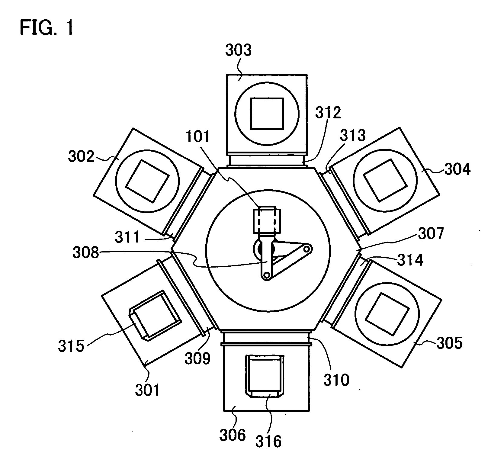
[0048]FIG. 1 illustrates an exemplary plasma treatment apparatus in accordance with the manufacture of a semiconductor device. The plasma treatment apparatus shown in FIG. 1 has a plurality of treatment chambers capable of generating plasma, a common chamber for transferring substrates to each chamber, and a load lock chamber for taking in or out the substrates. Thus, in the case of continuously performing deposition of an insulating film, a conductive layer, or a semiconductor layer and plasma treatment thereof, a plasma treatment apparatus having a plurality of treatment chambers can be used. Note that FIG. 1 is a top plan view showing one exemplary structure of a plasma treatment apparatus shown in this embodiment mode.

[0049] The plasma treatment chamber shown as an illustrative example in FIG. 1 includes a first treatment chamber 302, a second treatment chamber 303, a third treatment chamber 304, a fourth treatment chamber 305, load lock chambers 301 and 306, and a common chamb...

embodiment mode 2

[0069] A silicon oxide film which is deposited by plasma CVD with a parallel-plate chamber in which plasma is excited with a frequency of typically 13.56 MHz has a possibility that many defects are produced in the film due to the plasma damage or unreacted gas species during the film deposition. When transistors are manufactured by using such a silicon oxide film, various characteristics such as the threshold voltage or electron field-effect mobility are adversely affected.

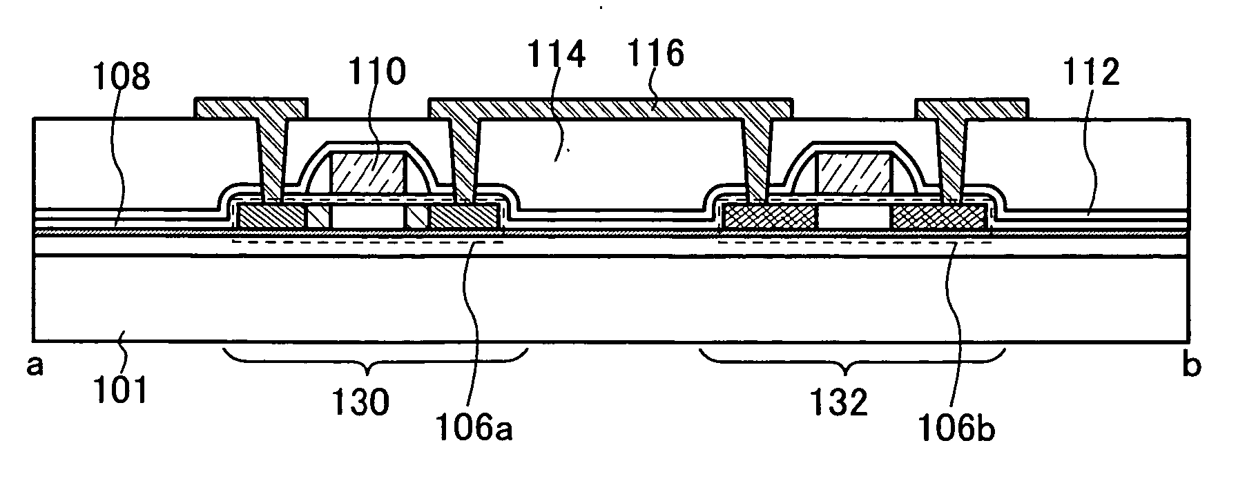
[0070] First, as shown in FIG. 4A, a silicon nitride film is formed with a thickness of 50 to 100 nm as a base insulating layer 102 over a substrate 101, by sputtering, low-pressure CVD, or plasma CVD. The silicon nitride film as the base insulating layer 102 is deposited at a substrate temperature of 250 to 400° C., or preferably 300 to 350° C. by supplying a gas of SiH4 and NH3 and / or N2. In this case, a silicon oxynitride film may be used instead of the silicon nitride film. The silicon oxynitride film can be ...

embodiment mode 3

[0079] An insulating layer formed between a glass substrate and a semiconductor layer in order to form a crystalline semiconductor layer is provided for the purpose of preventing diffusion of impurities from the substrate into the semiconductor layer as well as planarizing the surface of the glass substrate. Although a silicon nitride film is suitable for a blocking film which serves to prevent diffusion of impurities, it cannot be formed thick because of its high internal stress, so that it cannot increase the planarizing effect. In this embodiment mode, description will be made of an example of forming a base film by effectively using high-density plasma treatment, with reference to FIGS. 5A to 5E.

[0080] First, a substrate 101 is prepared, and the surface of the substrate 101 is cleaned with hydrofluoric acid (HF), alkali or pure water. The substrate 101 may be a glass substrate such as barium borosilicate glass, alumino borosilicate glass, or aluminosilicate glass, a quartz subs...


PUM


Abstract

To provide a semiconductor device having a circuit with high operating performance and high reliability, and improve the reliability of the semiconductor device, thereby improving the reliability of an electronic device having the same. The aforementioned object is achieved by combining a step of crystallizing a semiconductor layer by irradiation with continuous wave laser beams or pulsed laser beams with a repetition rate of 10 MHz or more, while scanning in one direction; a step of photolithography with the use of a photomask or a leticle including an auxiliary pattern which is formed of a diffraction grating pattern or a semi-transmissive film having a function of reducing the light intensity; and a step of performing oxidation, nitridation, or surface-modification to the surface of the semiconductor film, an insulating film, or a conductive film, with high-density plasma with a low electron temperature.

Description

BACKGROUND OF THE INVENTION [0001] 1. Field of the Invention [0002] The present invention relates to a semiconductor device and a manufacturing method thereof, which includes a step of performing plasma treatment to an insulating film or a semiconductor layer. [0003] 2. Description of the Related Art [0004] In recent years, techniques of forming a field-effect transistor (which includes a MOS transistor, a thin film transistor, an insulated-gate transistor, or the like; hereinafter also simply referred to as a “transistor”) by using a semiconductor thin film (with a thickness of about several nanometers to several hundred nanometers) formed over a substrate having an insulating surface such as glass, have been attracting attention. Transistors are widely applied to integrated circuits, liquid crystal display devices, and the like. Further, development of transistors with finer structures is demanded in accordance with the need for higher performance of electronic devices. [0005] It ...

Claims


Application Information

Patent Timeline
IPC IPC(8): G03F7/26
CPCH01L21/02238H01L21/02247H01L21/02252H01L27/1214H01L21/0234H01L21/2026H01L21/02332H01L27/1288H01L27/127H01L27/124H01L27/1285H01L21/02425H01L21/02683H01L21/02686H01L21/02502H01L21/02678H01L21/02422H01L21/02488H01L21/02532H01L21/0242H01L21/02691H01L21/3065
Inventor YAMAZAKI, SHUNPEIKAKEHATA, TETSUYAOHNUMA, HIDETONAGAI, MASAHARUOSAME, MITSUAKISAKAKURA, MASAYUKIKOMORI, SHIGEKI
Owner SEMICON ENERGY LAB CO LTD
Why Eureka
Try Eureka